LaTeX CircuiTikz Examples (I)
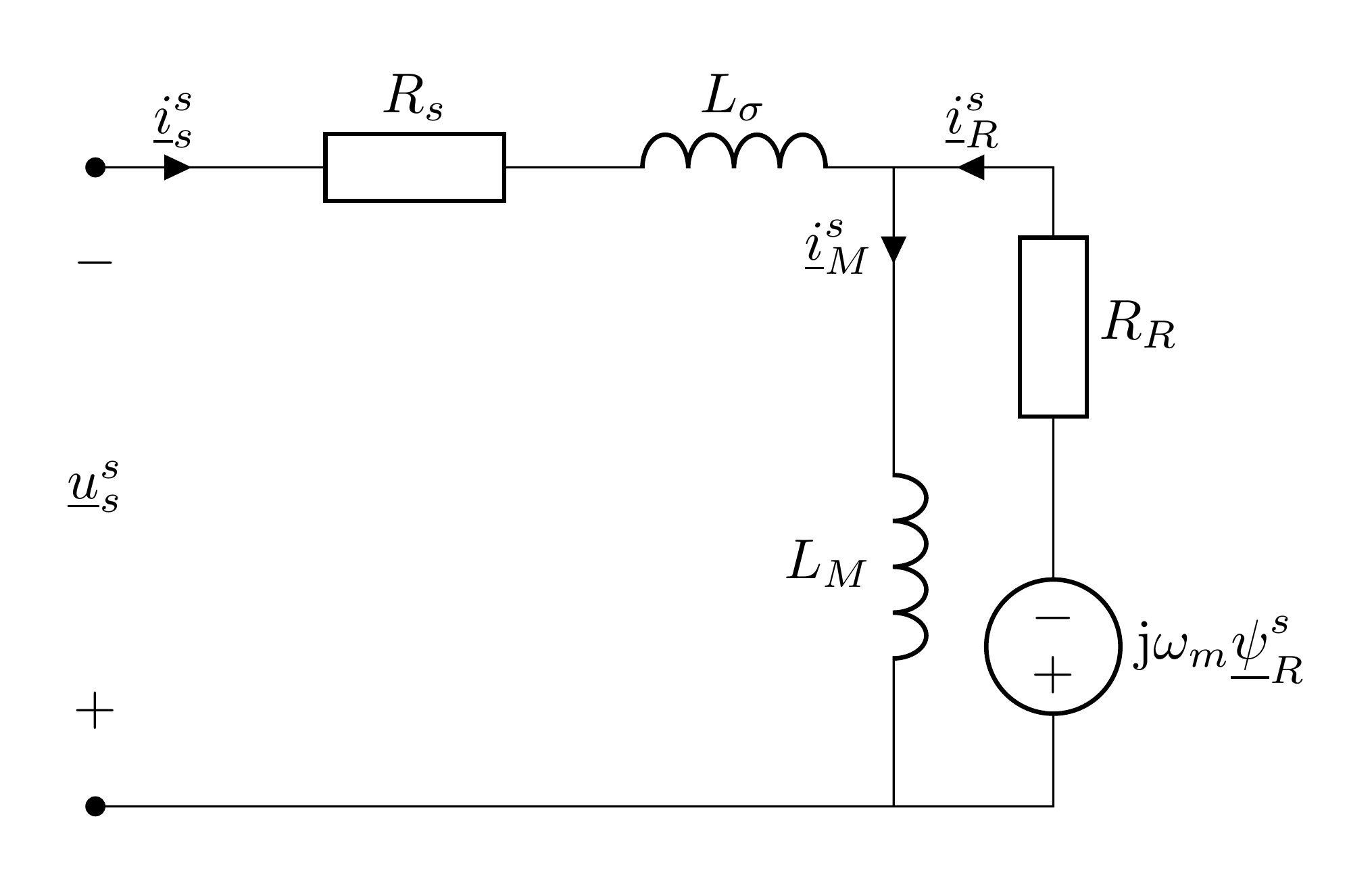
Example 1: Dynamic inverse-gamma-equivalent circuit for an induction machine
Example 1: Dynamic inverse-gamma-equivalent circuit for an induction machine1
1
2
3
4
5
6
7
8
9
10
11
12
13
14
15
16
17
18
19
20
21
22
23
24
25
26
27
28
29
% Dynamic inverse-$\varGamma$-equivalent circuit for an induction machine
% Author: Erno Pentzin (2013)
\documentclass{article}
\usepackage{tikz}
\usepackage[active,tightpage]{preview}
\PreviewEnvironment{tikzpicture}
\setlength\PreviewBorder{10pt}%
\usepackage[europeanresistors, americaninductors]{circuitikz}

\begin{document}

\begin{circuitikz}[american voltages]
	\draw
	  % rotor circuit
	  (0,0) to [short, *-] (6,0)
	  to [V, l_=$\mathrm{j}{\omega}_m \underline{\psi}^s_R$] (6,2) % rotor emf
	  to [R, l_=$R_R$] (6,4) % rotor resistance
	  to [short, i_=$\underline{i}^s_R$] (5,4) % rotor current

	  % stator circuit
	  (0,0) to [open, v^>=$\underline{u}^s_s$] (0,4) % stator voltage
	  to [short, *- ,i=$\underline{i}^s_s$] (1,4) % stator current
	  to [R, l=$R_s$] (3,4) % stator resistance
	  to [L, l=$L_{\sigma}$] (5,4) % leakage inductance
	  to [short, i_=$\underline{i}^s_M$] (5,3) % magnetizing current
	  to [L, l_=$L_M$] (5,0); % magnetizing inductance
\end{circuitikz}

\end{document}
Here is an annotated version to help understand this example.
1
2
3
4
5
6
7
8
9
10
11
12
13
14
15
16
17
18
19
20
21
22
23
24
25
26
27
28
29
30
31
32
33
34
35
36
37
38
39
40
41
42
% Dynamic inverse-$\varGamma$-equivalent circuit for an induction machine
% Author: Erno Pentzin (2013)
\documentclass{article}
\usepackage{tikz}
\usepackage[active,tightpage]{preview}
\PreviewEnvironment{tikzpicture}
\setlength\PreviewBorder{10pt}%
\usepackage[europeanresistors, americaninductors]{circuitikz}

\begin{document}

\begin{circuitikz}[american voltages]
	\draw [help lines,step=1cm] (0,0) grid (8,5); % Helper lines on the background

	\draw
	  % rotor circuit
	  (0,0) to [short, *-] (6,0)
	  to [V, l_=$\mathrm{j}{\omega}_m \underline{\psi}^s_R$] (6,2) % rotor emf
	  to [R, l_=$R_R$] (6,4) % rotor resistance
	  to [short, i_=$\underline{i}^s_R$] (5,4) % rotor current

	  % stator circuit
	  (0,0) to [open, v^>=$\underline{u}^s_s$] (0,4) % stator voltage
	  to [short, *- ,i=$\underline{i}^s_s$] (1,4) % stator current
	  to [R, l=$R_s$] (3,4) % stator resistance
	  to [L, l=$L_{\sigma}$] (5,4) % leakage inductance
	  to [short, i_=$\underline{i}^s_M$] (5,3) % magnetizing current
	  to [L, l_=$L_M$] (5,0); % magnetizing inductance

	  \fill [red] (0,0) circle (2pt) node[right=0.1cm, below=0.1cm]{(0,0)};
	  \fill [red] (6,0) circle (2pt) node[right=0.1cm]{(6,0)};
	  \fill [red] (6,2) circle (2pt) node[right=0.1cm]{(6,2)};
	  \fill [red] (6,4) circle (2pt) node[right=0.1cm]{(6,4)};
	  \fill [red] (5,4) circle (2pt) node[above=0.1cm]{(5,4)};
	  \fill [red] (0,4) circle (2pt) node[above=0.1cm]{(0,4)};
	  \fill [red] (1,4) circle (2pt) node[above=0.1cm]{(1,4)};
	  \fill [red] (3,4) circle (2pt) node[above=0.1cm]{(3,4)};
	  \fill [red] (5,3) circle (2pt) node[left=0.1cm]{(5,3)};
	  \fill [red] (5,0) circle (2pt) node[below=0.1cm]{(5,0)};
\end{circuitikz}

\end{document}

In this example, options europeanresistors and americaninductors of the circuitikz package and the american voltages of circuitikz environment are used to control element styles2. For example, if we change them as americanresistors, europeaninductors, and european voltages, respectively, we’ll have:
1
2
3
4
5
6
7
8
9
10
11
12
13
14
15
16
17
18
19
20
21
22
23
24
25
26
27
28
29
% Dynamic inverse-$\varGamma$-equivalent circuit for an induction machine
% Author: Erno Pentzin (2013)
\documentclass{article}
\usepackage{tikz}
\usepackage[active,tightpage]{preview}
\PreviewEnvironment{tikzpicture}
\setlength\PreviewBorder{10pt}%
\usepackage[americanresistors, europeaninductors]{circuitikz}

\begin{document}

\begin{circuitikz}[european voltages]
	\draw
	  % rotor circuit
	  (0,0) to [short, *-] (6,0)
	  to [V, l_=$\mathrm{j}{\omega}_m \underline{\psi}^s_R$] (6,2) % rotor emf
	  to [R, l_=$R_R$] (6,4) % rotor resistance
	  to [short, i_=$\underline{i}^s_R$] (5,4) % rotor current

	  % stator circuit
	  (0,0) to [open, v^>=$\underline{u}^s_s$] (0,4) % stator voltage
	  to [short, *- ,i=$\underline{i}^s_s$] (1,4) % stator current
	  to [R, l=$R_s$] (3,4) % stator resistance
	  to [L, l=$L_{\sigma}$] (5,4) % leakage inductance
	  to [short, i_=$\underline{i}^s_M$] (5,3) % magnetizing current
	  to [L, l_=$L_M$] (5,0); % magnetizing inductance
\end{circuitikz}

\end{document}
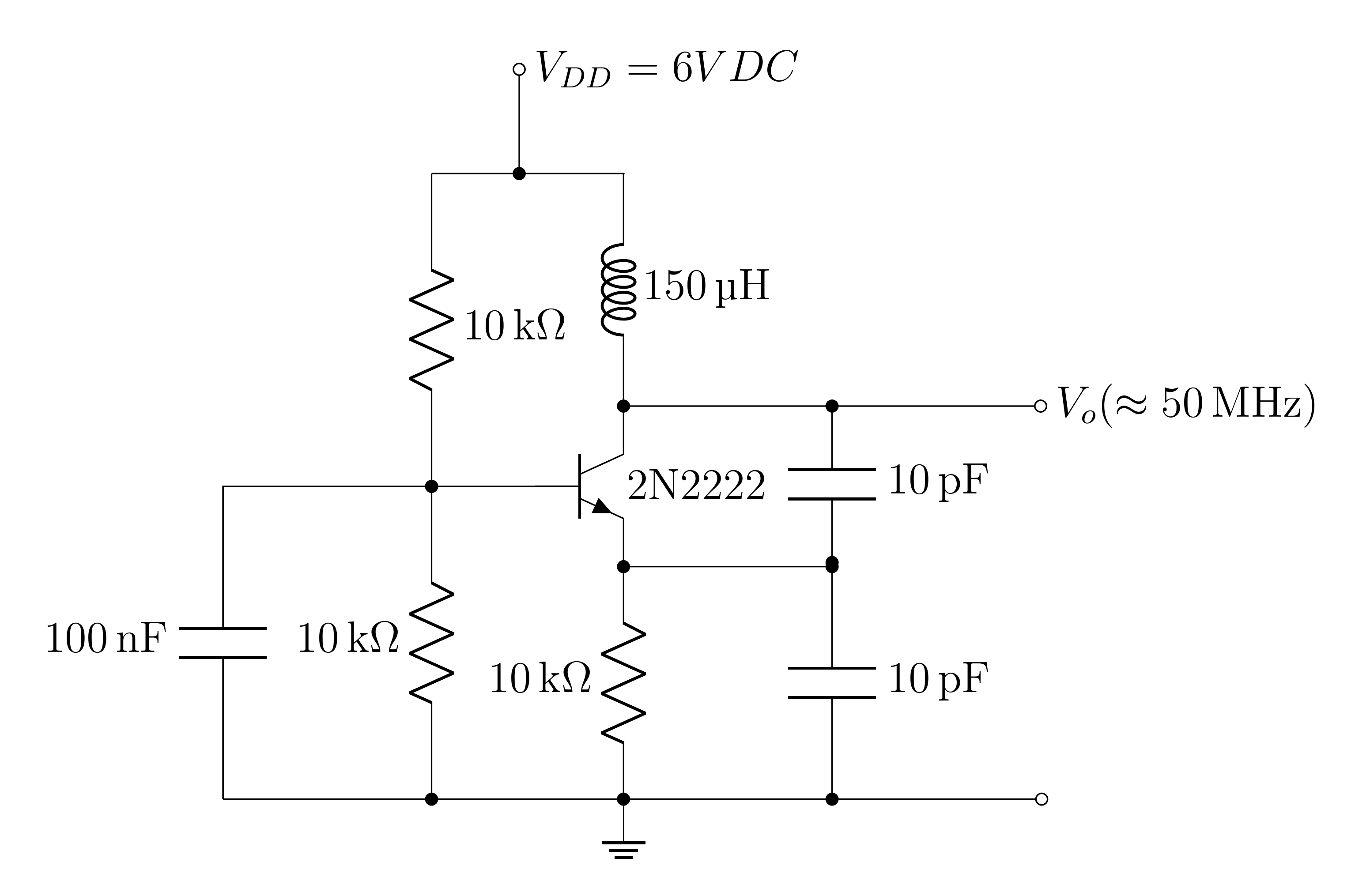
Example 2: Colpitts oscillator, with npn transistor
Example 2: Colpitts oscillator, with npn transistor3
1
2
3
4
5
6
7
8
9
10
11
12
13
14
15
16
17
18
19
20
21
22
23
24
25
26
27
28
29
% Title: Colpitts oscillator, with npn transistor
% Author: Ramón Jaramillo
\documentclass[tikz, border=10pt, 12pt]{standalone}% adequate for simple figures
\usepackage[siunitx]{circuitikz} % Loading circuitikz with siunitx option

\begin{document}
\begin{tikzpicture} % Or `circuitikz` environment
  \draw
	% Drawing a npn transistor
	(0,0) node[npn](npn1){}
	% Making connections from transistor using relative coordinates
	(npn1.E) node[right=7mm, above=5mm]{2N2222} % Labelling the transistor
	(npn1.B) -- ++(-1,0) to [R,l_=10<\kilo\ohm>,*-*] ++(0,-3)
	(npn1.B) -- ++(-3,0) to [C,l_=100<\nano\farad>] ++(0,-3) node(gnd1){}
	(npn1.E) to [R,l_=10<\kilo\ohm>,*-*] (0,-3)
	(npn1.E) -- ++(2,0) to [C,l=10<\pico\farad>,*-*] (2,-3)
	(npn1.B) -- ++(-1,0) to [R,l_=10<\kilo\ohm>,*-] ++(0,3) node(con1){} % -- ++(0.15,0)
	(npn1.C) to [L,l_=150<\micro\henry>,*-] (0,3)
	(npn1.C) -- ++(2,0) to [C,l=10<\pico\farad>,*-*] ++(0,-1.5)
	% Drawing shorts and ground connection
	(-1,3) to [short,*-o] (-1,4) node[right]{$V_{DD}=6 VDC$} % Power supply
	% Output sinusoidal waveform at approximately 50 MHz
	(npn1.C) -- ++(4,0) to [short,-o] ++(0,0) node[right]{$V_o (\approx \SI{50}{\MHz})$}
	(0,-3) node[ground]{} % Define this node as ground
	(gnd1) ++(0,0) to [short,-o] ++(7.85,0)
	(con1.center) to [short] ++(1.85,0) % Note "con1.center"
	;
\end{tikzpicture}
\end{document}
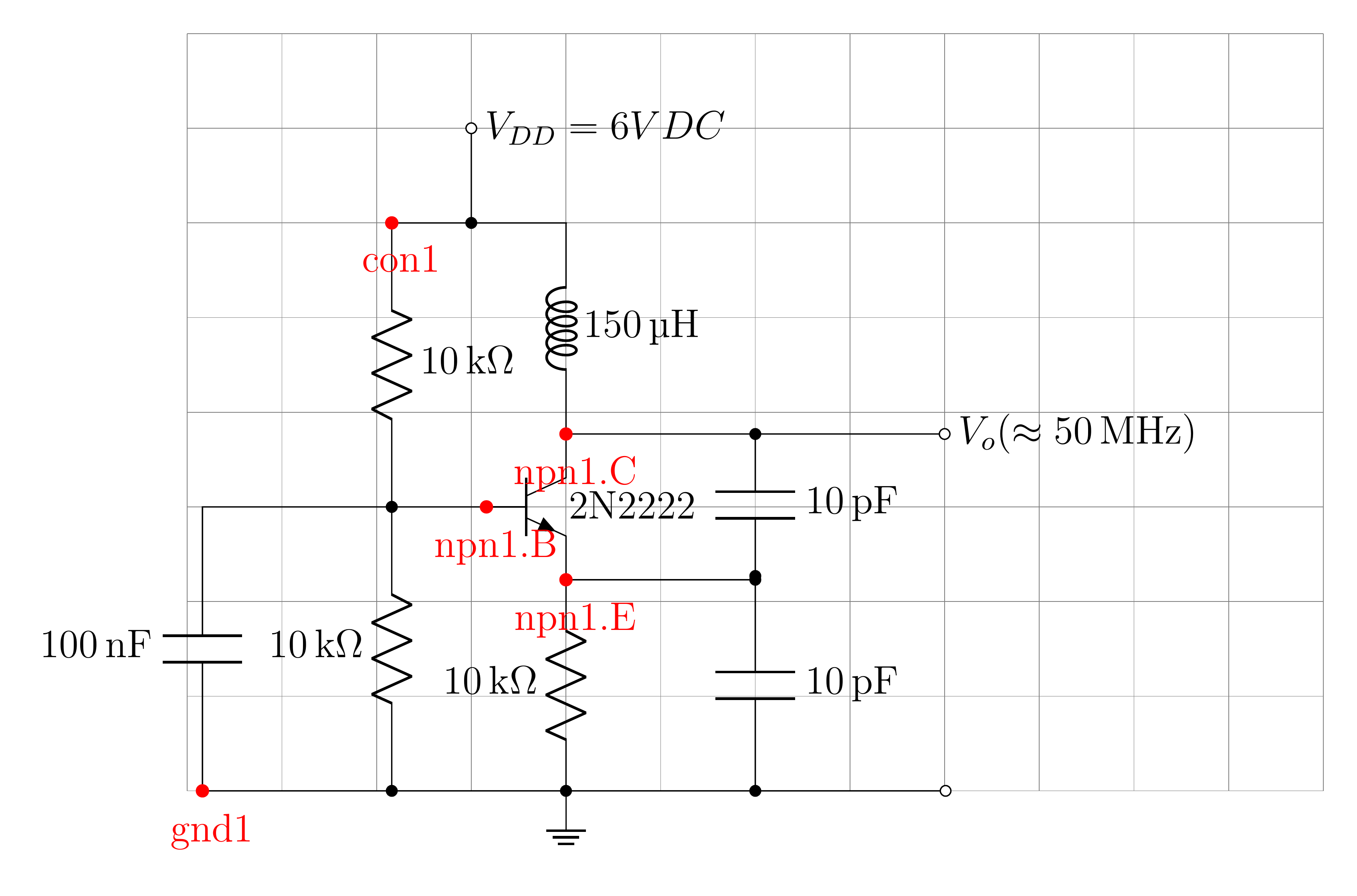
Here is an annotated version.
1
2
3
4
5
6
7
8
9
10
11
12
13
14
15
16
17
18
19
20
21
22
23
24
25
26
27
28
29
30
31
32
33
34
35
36
% Title: Colpitts oscillator, with npn transistor
% Author: Ramón Jaramillo
\documentclass[tikz, border=10pt, 12pt]{standalone}% adequate for simple figures
\usepackage[siunitx]{circuitikz} % Loading circuitikz with siunitx option

\begin{document}
\begin{tikzpicture} % Or `circuitikz` environment
  \draw [help lines,step=1cm] (-4,-3) grid (8,5); % Helper lines on the background
  \draw
	% Drawing a npn transistor
	(0,0) node[npn](npn1){}
	% Making connections from transistor using relative coordinates
	(npn1.E) node[right=7mm, above=5mm]{2N2222} % Labelling the transistor
	(npn1.B) -- ++(-1,0) to [R,l_=10<\kilo\ohm>,*-*] ++(0,-3)
	(npn1.B) -- ++(-3,0) to [C,l_=100<\nano\farad>] ++(0,-3) node(gnd1){}
	(npn1.E) to [R,l_=10<\kilo\ohm>,*-*] (0,-3)
	(npn1.E) -- ++(2,0) to [C,l=10<\pico\farad>,*-*] (2,-3)
	(npn1.B) -- ++(-1,0) to [R,l_=10<\kilo\ohm>,*-] ++(0,3) node(con1){} % -- ++(0.15,0)
	(npn1.C) to [L,l_=150<\micro\henry>,*-] (0,3)
	(npn1.C) -- ++(2,0) to [C,l=10<\pico\farad>,*-*] ++(0,-1.5)
	% Drawing shorts and ground connection
	(-1,3) to [short,*-o] (-1,4) node[right]{$V_{DD}=6 VDC$} % Power supply
	% Output sinusoidal waveform at approximately 50 MHz
	(npn1.C) -- ++(4,0) to [short,-o] ++(0,0) node[right]{$V_o (\approx \SI{50}{\MHz})$}
	(0,-3) node[ground]{} % Define this node as ground
	(gnd1) ++(0,0) to [short,-o] ++(7.85,0)
	(con1.center) to [short] ++(1.85,0) % Note "con1.center"
	;

	\fill [red] (npn1.E) circle (2pt) node[right=0.1cm, below=0.1cm]{npn1.E};
	\fill [red] (npn1.B) circle (2pt) node[right=0.1cm, below=0.1cm]{npn1.B};
	\fill [red] (npn1.C) circle (2pt) node[right=0.1cm, below=0.1cm]{npn1.C};
	\fill [red] (gnd1) circle (2pt) node[right=0.1cm, below=0.1cm]{gnd1};
	\fill [red] (con1) circle (2pt) node[right=0.1cm, below=0.1cm]{con1};
\end{tikzpicture}
\end{document}
(1) This example includes an NPN transistor (reference2, p. 114):
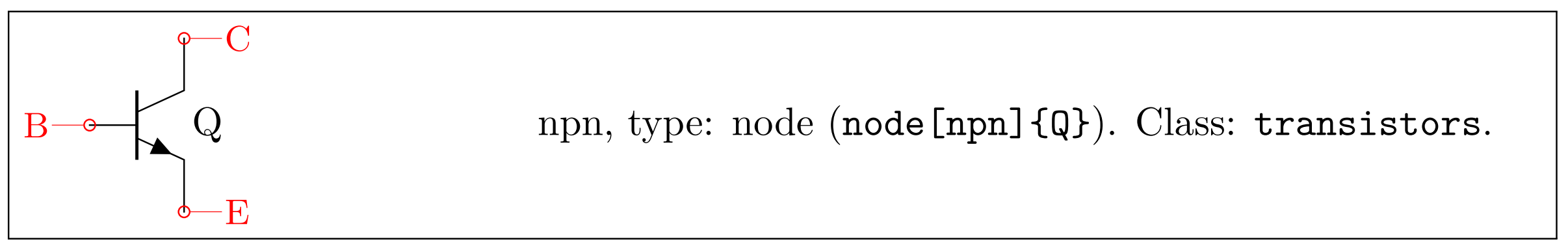
which includes three terminals, called as emitter (E), base (B), and collector (C)4. Also, more transistor styles (or, types) can be found in the CircuiTikZ manual (2, pp. 114-136).
(2) This example shows how to use relative coordinates in TikZ56, for example,
1
(npn1.B) -- ++(-1,0) to [R,l_=10<\kilo\ohm>,*-*] ++(0,-3)
where ++(-1,0) denotes the position that is away from (npn1.B) with distance (-1,0).
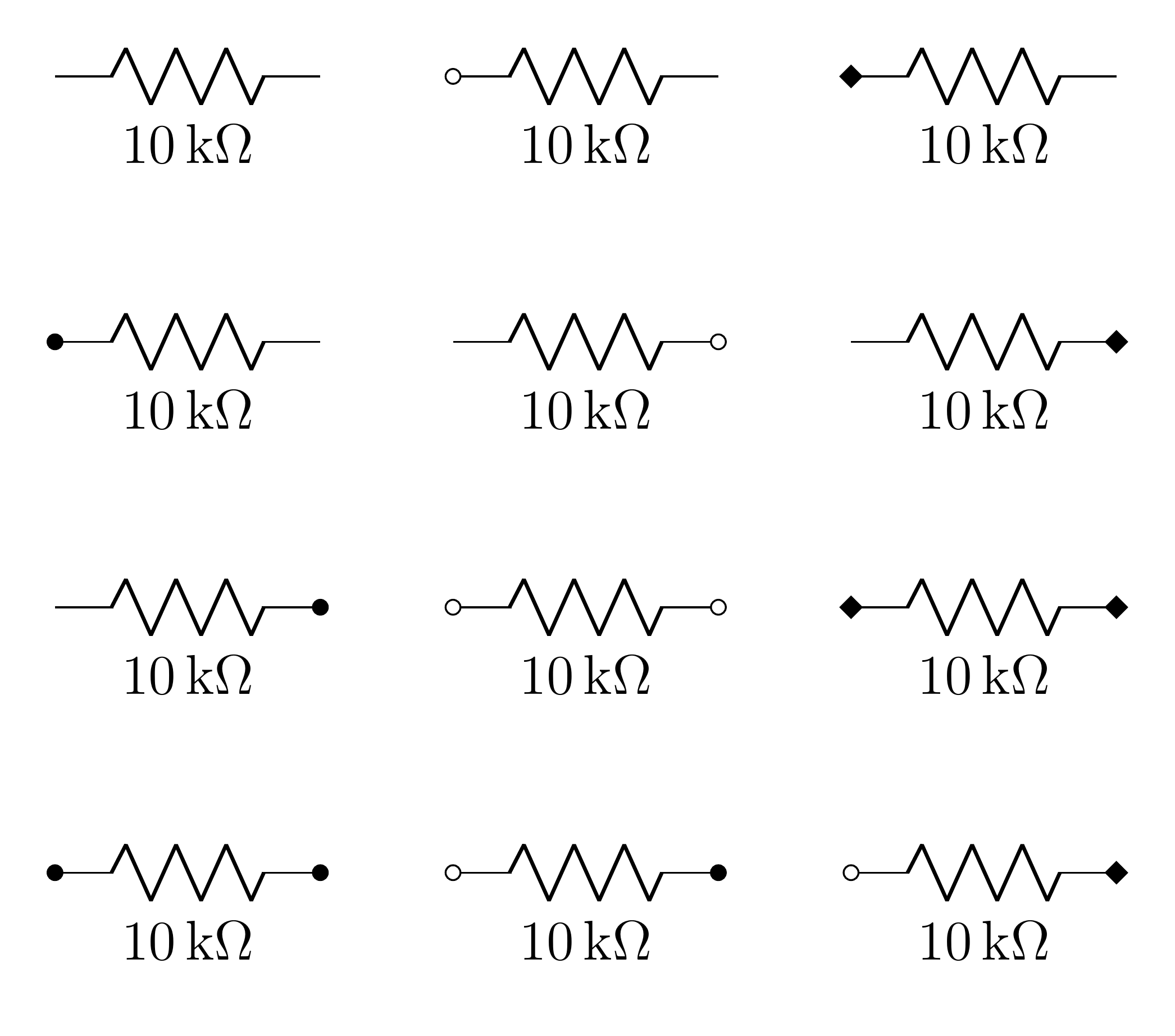
(3) The options like *-*, *-, *-o, and -o, are used to specify the style of line, where * and o are to specify the style of poles:
1
2
3
4
5
6
7
8
9
10
11
12
13
14
15
16
17
18
19
20
21
22
\documentclass[tikz, border=10pt, 12pt]{standalone}
\usepackage[siunitx]{circuitikz}

\begin{document}
\begin{tikzpicture}
  \draw (0,0) to [R,l_=10<\kilo\ohm>, -] ++(2,0);
  \draw (0,-2) to [R,l_=10<\kilo\ohm>, *-] ++(2,0);
  \draw (0,-4) to [R,l_=10<\kilo\ohm>, -*] ++(2,0);
  \draw (0,-6) to [R,l_=10<\kilo\ohm>, *-*] ++(2,0);


  \draw (3,0) to [R,l_=10<\kilo\ohm>, o-] ++(2,0);
  \draw (3,-2) to [R,l_=10<\kilo\ohm>, -o] ++(2,0);
  \draw (3,-4) to [R,l_=10<\kilo\ohm>, o-o] ++(2,0);
  \draw (3,-6) to [R,l_=10<\kilo\ohm>, o-*] ++(2,0);

  \draw (6,0) to [R,l_=10<\kilo\ohm>, d-] ++(2,0);
  \draw (6,-2) to [R,l_=10<\kilo\ohm>, -d] ++(2,0);
  \draw (6,-4) to [R,l_=10<\kilo\ohm>, d-d] ++(2,0);
  \draw (6,-6) to [R,l_=10<\kilo\ohm>, o-d] ++(2,0);
\end{tikzpicture}
\end{document}
More details can be found in the documentation(2, p. 99, pp. 233-234).
(4) Because the circuitikz package is imported with the option siunitx, i.e., \usepackage[siunitx]{circuitikz}, we can use those unit commands defined in the siunitx package, e.g., \ohm, \kilo\ohm, etc.
Example 3: 18W MOSFET amplifier with npn transistor
Example 3: 18W MOSFET amplifier with npn transistor7
1
2
3
4
5
6
7
8
9
10
11
12
13
14
15
16
17
18
19
20
21
22
23
24
25
26
27
28
29
30
31
32
33
34
35
36
37
38
39
40
41
42
43
44
45
46
% 18W MOSFET amplifier, with npn transistor.
% Author: Ramón Jaramillo.
\documentclass[tikz, border=10pt, 12pt]{standalone}
\usepackage[siunitx]{circuitikz}

\begin{document}
\begin{tikzpicture}[scale=2]
  \draw[color=black, thick]
    (0,0) to [short,o-] (6,0){} % Baseline for connection to ground
    % Input and ground
    (0,1) node[]{\large{\textbf{INPUT}}}
    % Connection of passive components
    (5,0) node[ground]{} node[circ](4.5,0){}
    (0,2) to [pC, l=$C_1$, o-] (0.5,2)
    to [R,l=$R_1$,](1.5,2)
    to node[short]{}(2.6,2)
    (1.5,2) to [C, l=$C_2$, *-] (1.5,3) -| (5,3)
    (2.2,2) to [R, l=$R_2$, *-*] (2.2,3)
    (2.2,3) to [pC, l=$C_3$, *-] (2.2,5) -| (3,5)
    % Transistor Bipolar Q1
    (3,0) to [R,l=$R_5$,-*] (3,1.5)
    to [Tnpn,n=npn1] (3,2.5)
    (npn1.E) node[right=3mm, above=5mm]{$Q_1$} % Labelling the NPN transistor
    (4,0) to [pC, l_=$C_4$, *-] (4, 1.5)--(3,1.5)
    (2.2,0) to [vR, l=$R_3$, *-*] (2.2,2)
    (3,2.5) to node[short]{}(3,3)
    (3,5) to [pR, n=pot1, l_=$R_4$, *-] (3,3)
    (3,5) to [R, l=$R_6$, *-] (5,5)
    to [short,*-o](5,5.5) node[right]{$V_S=40 V$}
    % Mosfet Transistors
    (5,3) to [Tnigfetd,n=mos1] (5,5)
    (mos1.B) node[anchor=west]{$Q_2$} % Labelling MOSFET Q2 Transistor
    (pot1.wiper)  to [R, l=$R_7$] (4.5,4) -| (mos1.G)
    (5,1.5) to [Tpigfetd,n=mos2] (5,2.5)
    (5,0) to (mos2.S)
    (3,2.5) to [R, l=$R_8$, *-] (4.5,2.5)
    -| (mos2.G)
    (mos2.B) node[anchor=west]{$Q_3$} % Labelling MOSFET Q3 Transistor
    % Output
    (6,3) to [pC, l=$C_5$,-*](5,3)
    (6,3) to [short,-o] (6,2){}
    (mos1.S)--(mos2.D)
    (6,0) to [short,-o] (6,1){} node[above=7mm]{\large{\textbf{SPEAKER}}}
    ;
\end{tikzpicture}
\end{document}
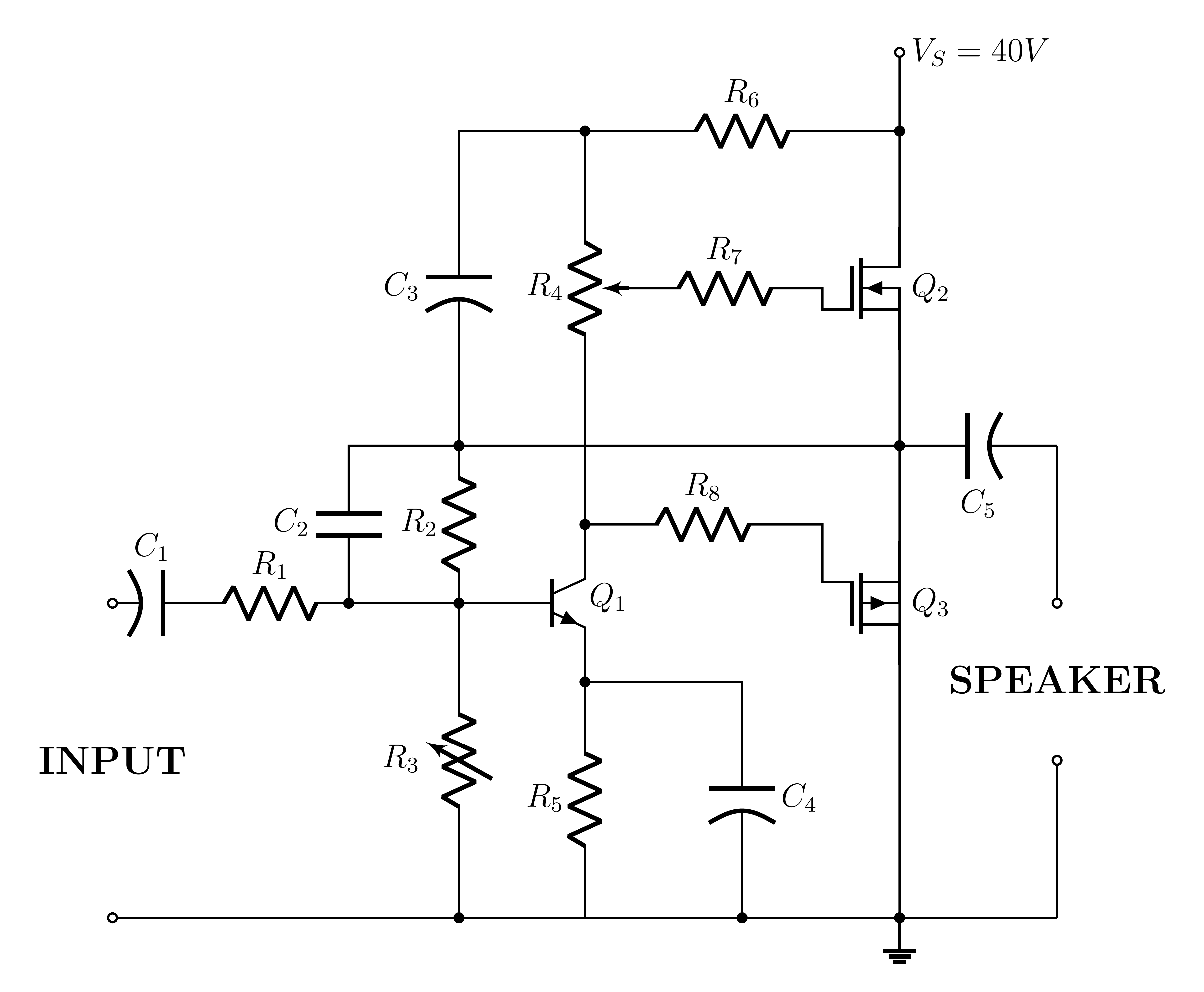
Here is an annotated version:
1
2
3
4
5
6
7
8
9
10
11
12
13
14
15
16
17
18
19
20
21
22
23
24
25
26
27
28
29
30
31
32
33
34
35
36
37
38
39
40
41
42
43
44
45
46
47
48
49
50
51
52
53
54
55
56
57
58
59
60
61
62
63
64
65
66
67
68
69
70
71
72
73
74
75
76
77
78
79
80
81
82
83
84
85
86
87
88
89
90
91
92
93
94
95
96
97
98
99
100
% 18W MOSFET amplifier, with npn transistor.
% Author: Ramón Jaramillo.
\documentclass[tikz, border=10pt, 12pt]{standalone}
\usepackage[siunitx]{circuitikz}

\begin{document}
\begin{tikzpicture}[scale=2]
  \draw [help lines,step=1cm] (0,0) grid (8,6); % Helper lines on the background

  \draw[color=black, thick]
    (0,0) to [short,o-] (6,0){} % Baseline for connection to ground
    % Input and ground
    (0,1) node[]{\large{\textbf{INPUT}}}
    % Connection of passive components
    (5,0) node[ground]{} node[circ](4.5,0){}
    (0,2) to [pC, l=$C_1$, o-] (0.5,2)
    to [R,l=$R_1$,](1.5,2)
    to node[short]{}(2.6,2)
    (1.5,2) to [C, l=$C_2$, *-] (1.5,3) -| (5,3)
    (2.2,2) to [R, l=$R_2$, *-*] (2.2,3)
    (2.2,3) to [pC, l=$C_3$, *-] (2.2,5) -| (3,5)
    % Transistor Bipolar Q1
    (3,0) to [R,l=$R_5$,-*] (3,1.5)
    to [Tnpn, n=npn1] (3,2.5)
    (npn1.E) node[right=3mm, above=5mm]{$Q_1$} % Labelling the NPN transistor
    (4,0) to [pC, l_=$C_4$, *-] (4, 1.5)--(3,1.5)
    (2.2,0) to [vR, l=$R_3$, *-*] (2.2,2)
    (3,2.5) to node[short]{}(3,3)
    (3,5) to [pR, n=pot1, l_=$R_4$, *-] (3,3)
    (3,5) to [R, l=$R_6$, *-] (5,5)
    to [short,*-o](5,5.5) node[right]{$V_S=40 V$}
    % Mosfet Transistors
    (5,3) to [Tnigfetd,n=mos1] (5,5)
    (mos1.B) node[anchor=west]{$Q_2$} % Labelling MOSFET Q2 Transistor
    (pot1.wiper)  to [R, l=$R_7$] (4.5,4) -| (mos1.G)
    (5,1.5) to [Tpigfetd,n=mos2] (5,2.5)
    (5,0) to (mos2.S)
    (3,2.5) to [R, l=$R_8$, *-] (4.5,2.5)
    -| (mos2.G)
    (mos2.B) node[anchor=west]{$Q_3$} % Labelling MOSFET Q3 Transistor
    % Output
    (6,3) to [pC, l=$C_5$,-*](5,3)
    (6,3) to [short,-o] (6,2){}
    (mos1.S)--(mos2.D)
    (6,0) to [short,-o] (6,1){} node[above=7mm]{\large{\textbf{SPEAKER}}}
    ;

	\fill [red] (0,0) circle (1pt) node[right=0.1cm, below=0.1cm]{(0,0)};
	\fill [red] (0,1) circle (1pt) node[right=0.1cm, below=0.1cm]{(0,1)};
	\fill [red] (0,2) circle (1pt) node[right=0.1cm, below=0.1cm]{(0,2)};

	\fill [red] (0.5,2) circle (1pt) node[right=0.1cm, below=0.1cm]{(0.5,2)};

	\fill [red] (1.5,2) circle (1pt) node[right=0.1cm, below=0.1cm]{(1.5,2)};
	\fill [red] (1.5,3) circle (1pt) node[right=0.1cm, above=0.1cm]{(1.5,3)};

	\fill [red] (2.2,0) circle (1pt) node[right=0.1cm, below=0.1cm]{(2.2,0)};
	\fill [red] (2.2,2) circle (1pt) node[right=0.1cm, above=0.05cm]{(2.2,2)};
	\fill [red] (2.2,3) circle (1pt) node[right=0.1cm, above=0.05cm]{(2.2,3)};
	\fill [red] (2.2,5) circle (1pt) node[right=0.1cm, above=0.05cm]{(2.2,5)};

	\fill [red] (2.6,2) circle (1pt) node[right=0.1cm, below=0.1cm]{(2.6,2)};

	\fill [red] (3,0) circle (1pt) node[right=0.1cm, below=0.1cm]{(3,0)};
	\fill [red] (3,1.5) circle (1pt) node[right=0.7cm, above=0.05cm]{(3,1.5)};
	\fill [red] (3,2.5) circle (1pt) node[right=0.1cm, above=0.05cm]{(3,2.5)};
	\fill [red] (3,3) circle (1pt) node[right=0.1cm, above=0.05cm]{(3,3)};
	\fill [red] (3,5) circle (1pt) node[right=0.1cm, above=0.05cm]{(3,5)};

	\fill [red] (4,0) circle (1pt) node[right=0.1cm, below=0.1cm]{(4,0)};
	\fill [red] (4,1.5) circle (1pt) node[right=0.1cm, below=0.1cm]{(4,1.5)};

	\fill [red] (4.5,2.5) circle (1pt) node[right=0.1cm, above=0.1cm]{(4.5,2.5)};
	\fill [red] (4.5,4) circle (1pt) node[right=0.1cm, above=0.1cm]{(4.5,4)};

	\fill [red] (5,0) circle (1pt) node[right=0.5cm, above=0.1cm]{(5,0)};
	\fill [red] (5,1.5) circle (1pt) node[right=0.1cm, below=0.1cm]{(5,1.5)};
	\fill [red] (5,2.5) circle (1pt) node[right=0.5cm, above=0.1cm]{(5,2.5)};
	\fill [red] (5,3) circle (1pt) node[right=0.1cm, above=0.1cm]{(5,3)};
	\fill [red] (5,5) circle (1pt) node[right=0.1cm, below=0.1cm]{(5,5)};

	\fill [red] (6,0) circle (1pt) node[right=0.1cm, below=0.1cm]{(6,0)};
	\fill [red] (6,1) circle (1pt) node[right=0.3cm]{(6,1)};
	\fill [red] (6,2) circle (1pt) node[right=0.3cm]{(6,2)};
	\fill [red] (6,3) circle (1pt) node[right=0.3cm]{(6,3)};

    \fill [blue] (npn1.E) circle (1pt) node[right=0.3cm]{npn1.E};

    \fill [blue] (mos1.S) circle (1pt) node[right=0.1cm]{mos1.S};
    \fill [blue] (mos1.B) circle (1pt) node[right=0.1cm]{mos1.B};
    \fill [blue] (mos1.G) circle (1pt) node[below=0.1cm]{mos1.G};

    \fill [blue] (mos2.S) circle (1pt) node[right=0.2cm]{mos2.S};
    \fill [blue] (mos2.G) circle (1pt) node[left=0.2cm]{mos2.G};
    \fill [blue] (mos2.B) circle (1pt) node[right=0.2cm]{mos2.B};
    \fill [blue] (mos2.D) circle (1pt) node[left=0.2cm]{mos2.D};

    \fill [blue] (pot1.wiper) circle (1pt) node[below=0.2cm]{pot1.wiper};
\end{tikzpicture}
\end{document}

In this example, the command -|8 are used three times:
1
2
3
4
5
6
7
    % ...
    (1.5,2) to [C, l=$C_2$, *-] (1.5,3) -| (5,3)
    % ...
    (2.2,3) to [pC, l=$C_3$, *-] (2.2,5) -| (3,5)
    % ...
    (pot1.wiper)  to [R, l=$R_7$] (4.5,4) -| (mos1.G)
    % ...
However, only the third one is functional — the first one and the second one are not, because (1.5,3) (resp. (2.2,5)) and (5,3) (resp. (3,5)) are on the same horizontal line, and hence -| can be simply replaced with --.
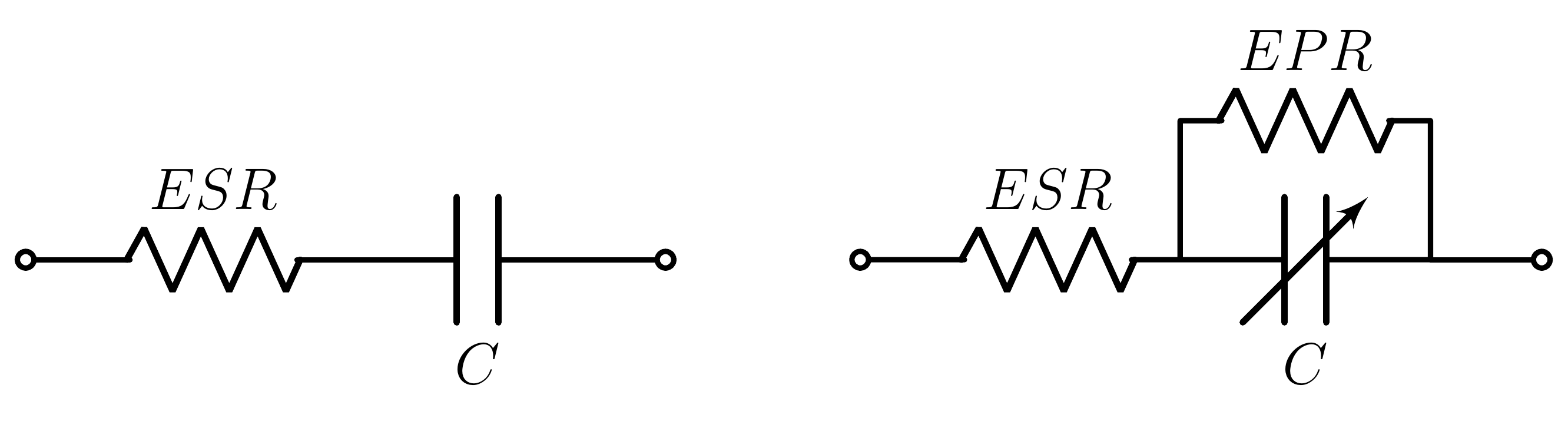
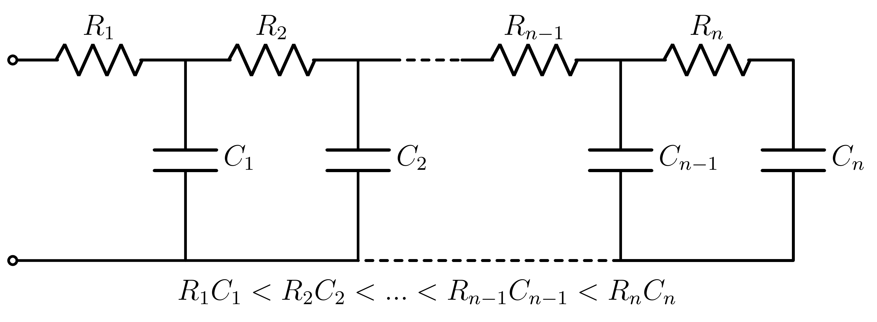
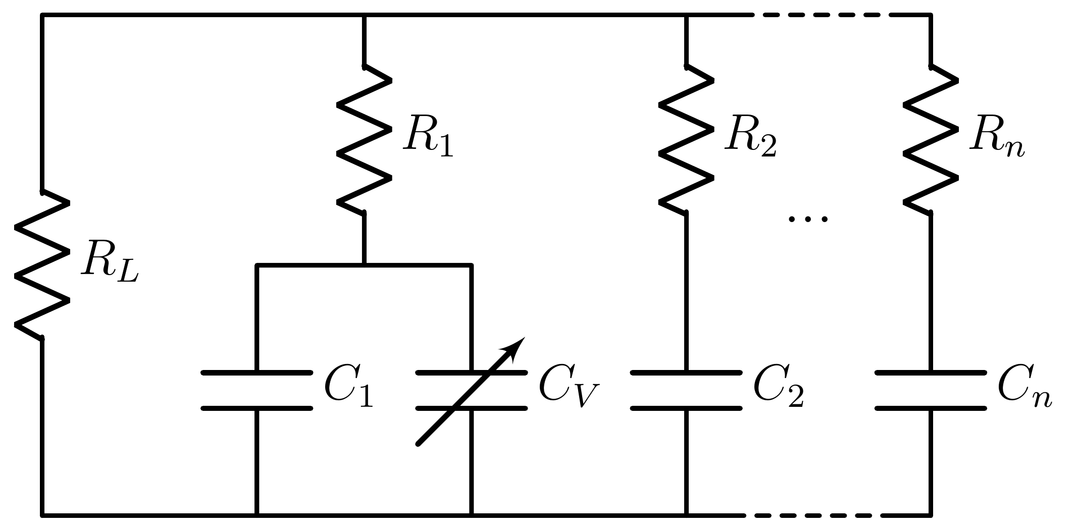
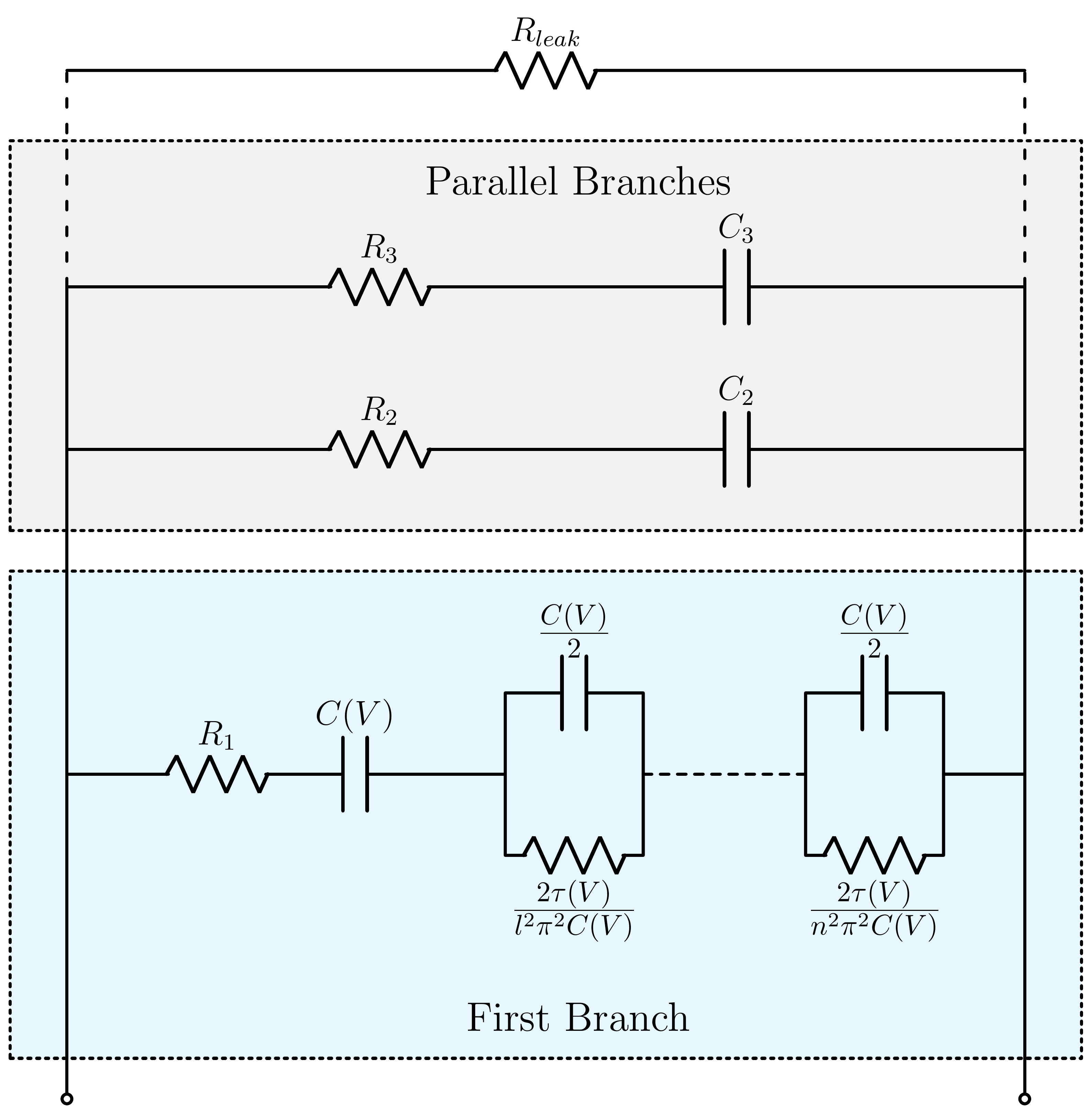
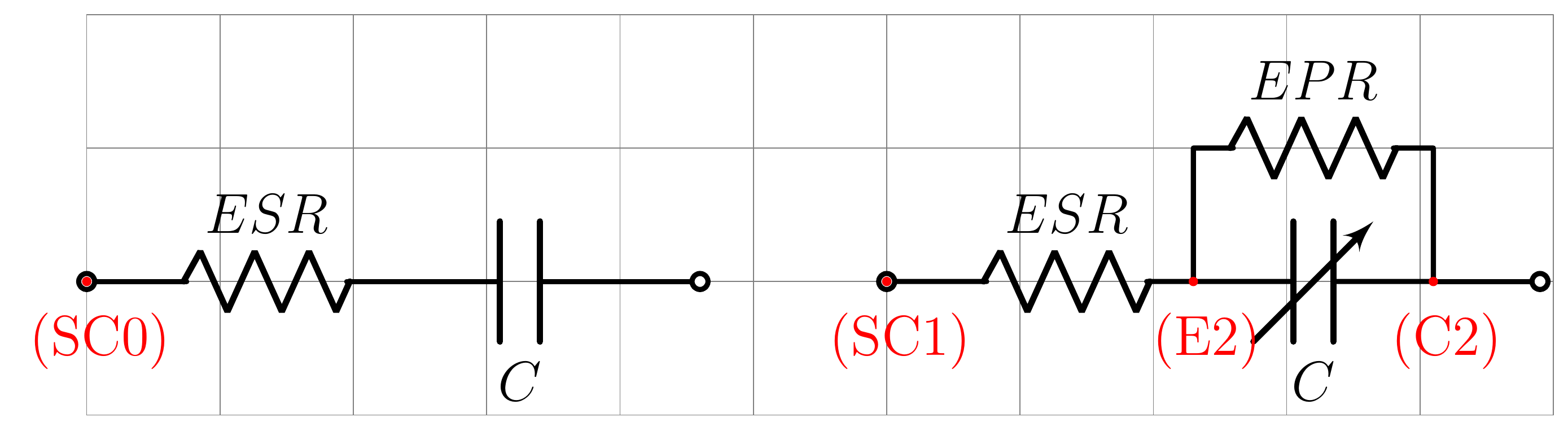
Example 4: Electrical Modeling of Supercapacitors
Example 4: Electrical Modeling of Supercapacitors9
1
2
3
4
5
6
7
8
9
10
11
12
13
14
15
16
17
18
19
20
21
22
23
24
25
26
27
28
29
30
31
32
33
34
35
36
37
38
39
40
41
42
43
44
45
46
47
48
49
50
51
52
53
54
55
56
57
58
59
60
61
62
63
64
65
66
67
68
69
70
71
72
73
74
75
76
77
78
79
80
81
82
83
84
85
86
87
88
89
90
91
92
93
94
95
96
97
98
99
100
101
102
103
104
105
106
107
108
109
110
111
112
113
114
 %Modeling of Supercapacitors (UltraCapacitors)
% Author: Amir Ostadrahimi
% for more information see: https://doi.org/10.1109/ACCESS.2023.3250965 --> ( New Parameter Identification Method for Supercapacitor Model )
\documentclass[border=3pt, tikz]{standalone}
\usepackage[american,cuteinductors,smartlabels]{circuitikz}
\ctikzset{bipoles/thickness=1.2}
\ctikzset{bipoles/length=1.5cm}
\tikzstyle{every node}=[font=\large]
\tikzstyle{every path}=[line width=1 .1pt,line cap=round,line join=round]

\begin{document}
\begin{tikzpicture}
	%Simple models of SCs
	%First Model (left)
	\coordinate (SC0) at (0,0) ;
	\draw (SC0) to [short,o-]++(0.4,0) to [R, l=$ESR$]++(1.9,0) to [C, l_=$C$]++(1.9,0) to [short,-o] ++(0.4,0);

	%Second Model (right)
	\coordinate (SC1) at (6,0) ;
	\draw (SC1) to [short,o-]++(0.4,0) to [R, l=$ESR$]++(1.9,0) coordinate (E2)
	to [short] ++(0,1) to [R, l=$EPR$] ++(1.8,0) to [short] ++(0,-1) coordinate (C2) to [vC, invert,mirror, l=$C$](E2);% using "mirror" and "invert" one can change the direction of the arrow.
	\draw (C2) to [short, -o]++(0.8,0);
\end{tikzpicture}

\begin{tikzpicture}
    %Transmission line Model
	\newcommand\gap{0.2} %short gap between elements
	\newcommand\Rlength{2.1} %length of resistors
	\newcommand\Clength{2.9} %length of Capacitors
	\coordinate (SC0) at (0,0) ;
	\draw (SC0) to [short,o-]++(\gap,0) to [R, l=$R_{1}$]++(\Rlength,0) to [short]++(\gap,0) coordinate (C1T); %% C1T is the point from which capacitor1 will be
	\draw (C1T) to [short]++(\gap,0) to [R, l=$R_{2}$]++(\Rlength,0) to[short]++(\gap,0) coordinate (C2T); %% C2T is the point from which capacitor1 will be
	\draw (C2T) --++(0.5,0) coordinate (dashedT1); %% dashed line in the top part of the circuit
	\draw [dashed] (dashedT1) --++ (1,0) coordinate (dashedT2); %% where dashed finishes in the top
	\draw (dashedT2) to [R, l=$R_{n-1}$]++(\Rlength,0) to [short]++(\gap,0) coordinate (CN1T) to[short]++(\gap,0) to [R, l=$R_{n}$]++(\Rlength,0) to [short]++(\gap,0) to [C, l=$C_{n}$]++(0,-\Clength) coordinate (CnB); %% CnB is the bottom of Cn
	%CAPACITORS
	\draw (C1T) to [C, l=$C_{1}$]++(0,-\Clength) coordinate (C1B); %% C1B is the bottom of C1
	\draw (C2T) to [C, l=$C_{2}$]++(0,-\Clength) coordinate (C2B); %% C2B is the bottom of C2
	\draw (CN1T) to [C, l=$C_{n-1}$]++(0,-\Clength) coordinate (CN1B); %% CN1B is the bottom of CN1
	\draw (SC0) to [open,] ++(0,-\Clength) coordinate (SC0B) ; %% SC0B is the bottoom part of the input
	% Lines
	\draw (CnB) -- (CN1B);
	\draw [dashed] (CN1B) -- (C2B);
	\draw (C2B) -- (C1B) to [short,-o] (SC0B);
	%description
	\coordinate [label={[xshift=0, yshift=0] \large $R_{1}C_{1}<R_{2}C_{2} <...<R_{n-1}C_{n-1}<R_{n}C_{n}$ }] (des) at (6,-3.7) ;
\end{tikzpicture}

\begin{tikzpicture}
    % Parallel model
	\newcommand\shortgap{0.9} %short gap between elements
	\newcommand\Rlength{2.1} %length of resistors
	\newcommand\Clength{2.9} %length of Capacitors
	\coordinate (SC0) at (0,0) ;
	\draw (SC0) to [R,l_=$R_{L}$] ++(0, 2*\Rlength) to [short] ++(3*\shortgap,0) coordinate (B2T); %% B2T is the top part of Branch 2
	\draw (B2T) to [R,l=$R_{1}$] ++(0, -\Rlength) coordinate (R1B) to [short] ++(-\shortgap,0) to [C, l=$C_{1}$] ++(0, -\Rlength) coordinate (C1B); %%R1B is bottom of the R1 and C1B is the top part of capacitor 1
	\draw (R1B) to [short]++(\shortgap,0) to [vC, invert, l=$C_{V}$] ++ (0,-\Rlength);
	\draw (B2T) to [short] ++(3*\shortgap,0) coordinate (B3T); %% B3T is the top part of Branch 3
	\draw (B3T)to [R,l=$R_{2}$]++ (0, -\Rlength) coordinate (mid1) to [C,l=$C_{2}$] ++ (0, -\Rlength) coordinate (B3B); %% B3B is the top part of Branch 3
	\draw (B3T) to [short] ++(0.5*\shortgap,0) coordinate (dashed1); %% dashed1 is the start of the dashed area
	\draw [dashed] (dashed1)--++(1.3,0) coordinate (dashed2); %% dashed 2 is the end of dashed area
	\draw (dashed2) to [short]++(0.3,0) to [R, l=$R_{n}$] ++(0, -\Rlength) coordinate (mid2) to [C, l=$C_{n}$]++(0,-\Rlength) coordinate (endd); %%endd is the end of the design
	\draw (endd) to [short]++(-0.3,0) coordinate (dashed2B);
	\draw [dashed] (dashed2B) -- ++(-1.3,0) coordinate (dashed1B);
	\draw (dashed1B) -- (SC0);
	\draw (mid1) to [open, l= \Large $...$] (mid2);
\end{tikzpicture}

\begin{tikzpicture}
	% Extended parallel model
	\newcommand\shgap{1} %short gap between elements
	\newcommand\Lgap{4} %large gap between elements
	\newcommand\Reslength{1.7} %length of resistors
	\newcommand\CapLength{1.7} %length of Capacitors
	\coordinate (SC0) at (0,0); %reference point
	%Rectangle1
	\draw (SC0) ++ (-0.7,0.5) coordinate (RE1LB); %RE1LB= Rectangle 1 left bottom
	\draw (SC0) ++ (12.5, 0.5) coordinate (RE1RB); %RE1LB= Rectangle 1 Right bottom
	\draw (RE1LB) ++ (0,1.5* \Lgap) coordinate (RE1LT); %RE1LB= Rectangle 1 left top
	\draw (RE1RB) ++ (0, 1.5* \Lgap) coordinate (RE1RT); %RE1LB= Rectangle 1 Right top
	\draw [ dotted, fill=cyan!10] (RE1LB)-- (RE1RB)-- (RE1RT) --(RE1LT) -- cycle;
	% Rectangle2
	\draw (SC0) ++ (-0.7,7) coordinate (RE1LB); %RE1LB= Rectangle 1 left bottom
	\draw (SC0) ++ (12.5, 7) coordinate (RE1RB); %RE1LB= Rectangle 1 Right bottom
	\draw (RE1LB) ++ (0, 1.2* \Lgap) coordinate (RE1LT); %RE1LB= Rectangle 1 left top
	\draw (RE1RB) ++ (0, 1.2* \Lgap) coordinate (RE1RT); %RE1LB= Rectangle 1 Right top
	\draw [ dotted, fill=gray!10] (RE1LB)-- (RE1RB)-- (RE1RT) --(RE1LT) -- cycle;
	%First Branch
	\draw (SC0) --++(0,\Lgap) coordinate (B1L); %% B1L is the left side of the branch 1
	\draw (B1L) to [short]++(\shgap,0) to [R, l=$R_{1}$]++(\Reslength,0) to [C, l=$C(V)$] ++(\CapLength,0) to [short]++(\shgap,0) coordinate (P1L); % P1L is the left side of the first parallel branch.
	\draw (P1L) to [short] ++ (0,1) to [C, l= \Large $\frac{C(V)}{2}$] ++(\CapLength,0) to [short] ++ (0,-1) coordinate (P1R); %% P1R is the right side of the parallel branch
	\draw (P1L) to [short] ++ (0,-1) to [R, l_= \Large $\frac{2\tau (V)}{l^{2} \pi ^{2} C(V)}$] ++(\CapLength,0) to [short] ++ (0,1);
	\draw [dashed] (P1R) --++(2,0) coordinate (P2L); % P1L is the left side of the first parallel branch.
	\draw (P2L) to [short] ++ (0,1) to [C, l= \Large $\frac{C(V)}{2}$] ++(\CapLength,0) to [short] ++ (0,-1) coordinate (P2R); %P2R is the right side of the second parallel branch
	\draw (P2L) to [short] ++ (0,-1) to [R, l_= \Large $\frac{2\tau (V)}{n^{2} \pi ^{2} C(V)}$] ++(\CapLength,0) to [short] ++ (0,1) to [short]++(1,0) coordinate (B1R); % B1R is the right side of the branch
	\draw (B1R) -- ++(0,-\Lgap) coordinate (SC1);
	\draw (SC0) to [open, o-o] (SC1);
	% Second Branch
	\draw (B1L)--++(0,\Lgap) coordinate (B2L); % B2L is the left side of the second branch
	\draw (B1R)--++(0,\Lgap) coordinate (B2R); % B2R is the right side of the second branch
	\draw (B2L) to [short] ++(3*\shgap,0) to [R, l=$R_{2}$]++(\Reslength,0) to [C, l=$C_{2}$] (B2R);
	%Third Branch
	\draw (B2L)--++(0,\Lgap/2) coordinate (B3L); % B3L is the left side of the third branch
	\draw (B2R)--++(0,\Lgap/2) coordinate (B3R); % B3R is the right side of the third branch
	\draw (B3L) to [short] ++(3*\shgap,0) to [R, l=$R_{3}$]++(\Reslength,0) to [C, l=$C_{3}$] (B3R);
	%Fourth Branch
	\draw [loosely dashed] (B3L)--++(0,\Lgap/1.5) coordinate (B4L); % B4L is the left side of the fourth branch
	\draw [loosely dashed] (B3R)--++(0,\Lgap/1.5) coordinate (B4R); % B4R is the right side of the fourth branch
	\draw (B4L) to [R, l=$R_{leak}$] (B4R);
	%Descriptions
	\coordinate [ label={ \Large First Branch}] (DES1) at (6.3,0.7);
	\coordinate [ label={ \Large Parallel Branches }] (DES1) at (6.3,11);
\end{tikzpicture}
\end{document}
Here is an annotated version:
1
2
3
4
5
6
7
8
9
10
11
12
13
14
15
16
17
18
19
20
21
22
23
24
25
26
27
28
29
30
31
32
33
34
35
36
37
38
39
40
41
42
43
44
45
46
47
48
49
50
51
52
53
54
55
56
57
58
59
60
61
62
63
64
65
66
67
68
69
70
71
72
73
74
75
76
77
78
79
80
81
82
83
84
85
86
87
88
89
90
91
92
93
94
95
96
97
98
99
100
101
102
103
104
105
106
107
108
109
110
111
112
113
114
115
116
117
118
119
120
121
122
123
124
125
126
127
128
129
130
131
132
133
134
135
136
137
138
139
140
141
142
143
144
145
146
147
148
149
150
151
152
153
154
155
156
157
158
159
160
161
162
163
164
165
166
167
168
169
170
171
172
173
174
175
176
177
178
179
180
181
182
183
184
185
186
%Modeling of Supercapacitors (UltraCapacitors)
% Author: Amir Ostadrahimi
% for more information see: https://doi.org/10.1109/ACCESS.2023.3250965 --> ( New Parameter Identification Method for Supercapacitor Model )
\documentclass[border=3pt, tikz]{standalone}
\usepackage[american,cuteinductors,smartlabels]{circuitikz}
\ctikzset{bipoles/thickness=1.2}
\ctikzset{bipoles/length=1.5cm}
\tikzstyle{every node}=[font=\large]
\tikzstyle{every path}=[line width=1 .1pt,line cap=round,line join=round]

\begin{document}
\begin{tikzpicture}
	\draw [help lines,step=1cm] (0,-1) grid (11,2); % Helper lines on the background

	%Simple models of SCs
	%First Model (left)
	\coordinate (SC0) at (0,0) ;
	\draw (SC0) to [short,o-]++(0.4,0) to [R, l=$ESR$] ++(1.9,0) to [C, l_=$C$] ++(1.9,0) to [short,-o] ++(0.4,0);

	%Second Model (right)
	\coordinate (SC1) at (6,0) ;
	\draw (SC1) to [short,o-]++(0.4,0) to [R, l=$ESR$]++(1.9,0) coordinate (E2)
	to [short] ++(0,1) to [R, l=$EPR$] ++(1.8,0) to [short] ++(0,-1) coordinate (C2) to [vC, invert, mirror, l=$C$](E2);% using "mirror" and "invert" one can change the direction of the arrow.
	\draw (C2) to [short, -o]++(0.8,0);

	\fill [red] (SC0) circle (1pt) node[right=0.1cm, below=0.1cm]{(SC0)};
	\fill [red] (SC1) circle (1pt) node[right=0.1cm, below=0.1cm]{(SC1)};
	\fill [red] (C2) circle (1pt) node[right=0.1cm, below=0.1cm]{(C2)};
	\fill [red] (E2) circle (1pt) node[right=0.1cm, below=0.1cm]{(E2)};
\end{tikzpicture}

\begin{tikzpicture}
	\draw [help lines,step=1cm] (0,-4) grid (13,1); % Helper lines on the background

    %Transmission line Model
	\newcommand\gap{0.2} %short gap between elements
	\newcommand\Rlength{2.1} %length of resistors
	\newcommand\Clength{2.9} %length of Capacitors
	\coordinate (SC0) at (0,0) ;
	\draw (SC0) to [short,o-]++(\gap,0) to [R, l=$R_{1}$]++(\Rlength,0) to [short]++(\gap,0) coordinate (C1T); %% C1T is the point from which capacitor1 will be
	\draw (C1T) to [short]++(\gap,0) to [R, l=$R_{2}$]++(\Rlength,0) to[short]++(\gap,0) coordinate (C2T); %% C2T is the point from which capacitor1 will be
	\draw (C2T) --++(0.5,0) coordinate (dashedT1); %% dashed line in the top part of the circuit
	\draw [dashed] (dashedT1) --++ (1,0) coordinate (dashedT2); %% where dashed finishes in the top
	\draw (dashedT2) to [R, l=$R_{n-1}$]++(\Rlength,0) to [short]++(\gap,0) coordinate (CN1T) to[short]++(\gap,0) to [R, l=$R_{n}$]++(\Rlength,0) to [short]++(\gap,0) to [C, l=$C_{n}$]++(0,-\Clength) coordinate (CnB); %% CnB is the bottom of Cn
	%CAPACITORS
	\draw (C1T) to [C, l=$C_{1}$]++(0,-\Clength) coordinate (C1B); %% C1B is the bottom of C1
	\draw (C2T) to [C, l=$C_{2}$]++(0,-\Clength) coordinate (C2B); %% C2B is the bottom of C2
	\draw (CN1T) to [C, l=$C_{n-1}$]++(0,-\Clength) coordinate (CN1B); %% CN1B is the bottom of CN1
	\draw (SC0) to [open,] ++(0,-\Clength) coordinate (SC0B) ; %% SC0B is the bottoom part of the input
	% Lines
	\draw (CnB) -- (CN1B);
	\draw [dashed] (CN1B) -- (C2B);
	\draw (C2B) -- (C1B) to [short,-o] (SC0B);
	%description
	\coordinate [label={[xshift=0, yshift=0] \large $R_{1}C_{1}<R_{2}C_{2} <...<R_{n-1}C_{n-1}<R_{n}C_{n}$ }] (des) at (6,-3.7);

	\fill [red] (SC0) circle (1pt) node[right=0.1cm, below=0.1cm]{(SC0)};
	\fill [red] (C1T) circle (1pt) node[right=0.1cm, below=0.1cm]{(C1T)};
	\fill [red] (C2T) circle (1pt) node[right=0.1cm, below=0.1cm]{(C2T)};
	\fill [blue] (dashedT1) circle (1pt) node[right=0.1cm, above=0.1cm]{(dashedT1)};
	\fill [blue] (dashedT2) circle (1pt) node[right=0.1cm, below=0.3cm]{(dashedT2)};
	\fill [red] (CN1T) circle (1pt) node[right=0.1cm, below=0.1cm]{(CN1T)};
	\fill [red] (C1B) circle (1pt) node[right=0.1cm, above=0.1cm]{(C1B)};
	\fill [red] (C2B) circle (1pt) node[right=0.1cm, above=0.1cm]{(C2B)};
	\fill [red] (CN1B) circle (1pt) node[right=0.1cm, above=0.1cm]{(CN1B)};
	\fill [red] (SC0B) circle (1pt) node[right=0.1cm, above=0.1cm]{(SC0B)};
	\fill [red] (CnB) circle (1pt) node[right=0.1cm, above=0.1cm]{(CnB)};
	\fill [red] (des) circle (1pt) node[right=0.1cm, below=0.1cm]{(des)};
\end{tikzpicture}

\begin{tikzpicture}
	\draw [help lines,step=1cm] (0,-1) grid (9,5); % Helper lines on the background

    % Parallel model
	\newcommand\shortgap{0.9} %short gap between elements
	\newcommand\Rlength{2.1} %length of resistors
	\newcommand\Clength{2.9} %length of Capacitors
	\coordinate (SC0) at (0,0) ;
	\draw (SC0) to [R,l_=$R_{L}$] ++(0, 2*\Rlength) to [short] ++(3*\shortgap,0) coordinate (B2T); %% B2T is the top part of Branch 2
	\draw (B2T) to [R,l=$R_{1}$] ++(0, -\Rlength) coordinate (R1B) to [short] ++(-\shortgap,0) to [C, l=$C_{1}$] ++(0, -\Rlength) coordinate (C1B); %%R1B is bottom of the R1 and C1B is the top part of capacitor 1
	\draw (R1B) to [short]++(\shortgap,0) to [vC, invert, l=$C_{V}$] ++ (0,-\Rlength);
	\draw (B2T) to [short] ++(3*\shortgap,0) coordinate (B3T); %% B3T is the top part of Branch 3
	\draw (B3T) to [R,l=$R_{2}$]++ (0, -\Rlength) coordinate (mid1) to [C,l=$C_{2}$] ++ (0, -\Rlength) coordinate (B3B); %% B3B is the top part of Branch 3
	\draw (B3T) to [short] ++(0.5*\shortgap,0) coordinate (dashed1); %% dashed1 is the start of the dashed area
	\draw [dashed] (dashed1) -- ++(1.3,0) coordinate (dashed2); %% dashed 2 is the end of dashed area
	\draw (dashed2) to [short]++(0.3,0) to [R, l=$R_{n}$] ++(0, -\Rlength) coordinate (mid2) to [C, l=$C_{n}$] ++(0,-\Rlength) coordinate (endd); %%endd is the end of the design
	\draw (endd) to [short] ++(-0.3,0) coordinate (dashed2B);
	\draw [dashed] (dashed2B) -- ++(-1.3,0) coordinate (dashed1B);
	\draw (dashed1B) -- (SC0);
	\draw (mid1) to [open, l= \Large $...$] (mid2);

	\fill [red] (SC0) circle (1pt) node[right=0.1cm, below=0.1cm]{(SC0)};
	\fill [red] (B2T) circle (1pt) node[right=0.1cm, above=0.1cm]{(B2T)};
	\fill [red] (C1B) circle (1pt) node[right=0.1cm, below=0.1cm]{(C1B)};
	\fill [red] (R1B) circle (1pt) node[right=0.7cm, above=0.1cm]{(R1B)};
	\fill [red] (B3T) circle (1pt) node[right=0.1cm, above=0.1cm]{(B3T)};
	\fill [red] (B3B) circle (1pt) node[right=0.1cm, above=0.1cm]{(B3B)};
	\fill [blue] (dashed1) circle (1pt) node[right=0.1cm, below=0.1cm]{(dashed1)};
	\fill [blue] (dashed2) circle (1pt) node[right=0.1cm, above=0.1cm]{(dashed2)};
	\fill [red] (endd) circle (1pt) node[right=0.1cm, below=0.1cm]{(endd)};
	\fill [blue] (dashed1B) circle (1pt) node[right=0.1cm, below=0.1cm]{(dashed1B)};
	\fill [blue] (dashed2B) circle (1pt) node[right=0.1cm, above=0.1cm]{(dashed2B)};
	\fill [red] (mid1) circle (1pt) node[right=0.1cm, below=0.1cm]{(mid1)};
	\fill [red] (mid2) circle (1pt) node[right=0.1cm, below=0.1cm]{(mid2)};
\end{tikzpicture}

\begin{tikzpicture}
	\draw [help lines,step=1cm] (-1,-1) grid (13,13); % Helper lines on the background

	% Extended parallel model
	\newcommand\shgap{1} %short gap between elements
	\newcommand\Lgap{4} %large gap between elements
	\newcommand\Reslength{1.7} %length of resistors
	\newcommand\CapLength{1.7} %length of Capacitors
	\coordinate (SC0) at (0,0); %reference point

	%Rectangle1
	\draw (SC0) ++ (-0.7,0.5) coordinate (RE1LB); %RE1LB= Rectangle 1 left bottom
	\draw (SC0) ++ (12.5, 0.5) coordinate (RE1RB); %RE1LB= Rectangle 1 Right bottom
	\draw (RE1LB) ++ (0,1.5* \Lgap) coordinate (RE1LT); %RE1LB= Rectangle 1 left top
	\draw (RE1RB) ++ (0, 1.5* \Lgap) coordinate (RE1RT); %RE1LB= Rectangle 1 Right top
	\draw [dotted, fill=cyan!10] (RE1LB) -- (RE1RB) -- (RE1RT) -- (RE1LT) -- cycle;

	% Rectangle2
	\draw (SC0) ++ (-0.7,7) coordinate (RE1LB); %RE1LB= Rectangle 1 left bottom
	\draw (SC0) ++ (12.5, 7) coordinate (RE1RB); %RE1LB= Rectangle 1 Right bottom
	\draw (RE1LB) ++ (0, 1.2* \Lgap) coordinate (RE1LT); %RE1LB= Rectangle 1 left top
	\draw (RE1RB) ++ (0, 1.2* \Lgap) coordinate (RE1RT); %RE1LB= Rectangle 1 Right top
	\draw [dotted, fill=gray!10] (RE1LB)-- (RE1RB)-- (RE1RT) --(RE1LT) -- cycle;

	%First Branch
	\draw (SC0) --++(0,\Lgap) coordinate (B1L); %% B1L is the left side of the branch 1
	\draw (B1L) to [short] ++(\shgap,0) to [R, l=$R_{1}$]++(\Reslength,0) to [C, l=$C(V)$] ++(\CapLength,0) to [short] ++(\shgap,0) coordinate (P1L); % P1L is the left side of the first parallel branch.
	\draw (P1L) to [short] ++ (0,1) to [C, l= \Large $\frac{C(V)}{2}$] ++(\CapLength,0) to [short] ++ (0,-1) coordinate (P1R); %% P1R is the right side of the parallel branch
	\draw (P1L) to [short] ++ (0,-1) to [R, l_= \Large $\frac{2\tau (V)}{l^{2} \pi ^{2} C(V)}$] ++(\CapLength,0) to [short] ++ (0,1);
	\draw [dashed] (P1R) --++(2,0) coordinate (P2L); % P1L is the left side of the first parallel branch.
	\draw (P2L) to [short] ++ (0,1) to [C, l= \Large $\frac{C(V)}{2}$] ++(\CapLength,0) to [short] ++ (0,-1) coordinate (P2R); %P2R is the right side of the second parallel branch
	\draw (P2L) to [short] ++ (0,-1) to [R, l_= \Large $\frac{2\tau (V)}{n^{2} \pi ^{2} C(V)}$] ++(\CapLength,0) to [short] ++ (0,1) to [short]++(1,0) coordinate (B1R); % B1R is the right side of the branch
	\draw (B1R) -- ++(0,-\Lgap) coordinate (SC1);
	\draw (SC0) to [open, o-o] (SC1);

	% Second Branch
	\draw (B1L)--++(0,\Lgap) coordinate (B2L); % B2L is the left side of the second branch
	\draw (B1R)--++(0,\Lgap) coordinate (B2R); % B2R is the right side of the second branch
	\draw (B2L) to [short] ++(3*\shgap,0) to [R, l=$R_{2}$]++(\Reslength,0) to [C, l=$C_{2}$] (B2R);

	%Third Branch
	\draw (B2L)--++(0,\Lgap/2) coordinate (B3L); % B3L is the left side of the third branch
	\draw (B2R)--++(0,\Lgap/2) coordinate (B3R); % B3R is the right side of the third branch
	\draw (B3L) to [short] ++(3*\shgap,0) to [R, l=$R_{3}$]++(\Reslength,0) to [C, l=$C_{3}$] (B3R);

	%Fourth Branch
	\draw [loosely dashed] (B3L)--++(0,\Lgap/1.5) coordinate (B4L); % B4L is the left side of the fourth branch
	\draw [loosely dashed] (B3R)--++(0,\Lgap/1.5) coordinate (B4R); % B4R is the right side of the fourth branch
	\draw (B4L) to [R, l=$R_{leak}$] (B4R);

	%Descriptions
	\coordinate [label={ \Large First Branch}] (DES1) at (6.3,0.7);
	\coordinate [label={ \Large Parallel Branches}] (DES2) at (6.3,11);

	\fill [red] (RE1LB) circle (1pt) node[right=0.1cm, above=0.1cm]{(RE1LB)};
	\fill [red] (RE1RB) circle (1pt) node[right=0.1cm, above=0.1cm]{(RE1RB)};
	\fill [red] (RE1LT) circle (1pt) node[right=0.1cm, below=0.1cm]{(RE1LT)};
	\fill [red] (RE1RT) circle (1pt) node[right=0.1cm, below=0.1cm]{(RE1RT)};

	\fill [red] (SC0) circle (1pt) node[right=0.1cm, below=0.1cm]{(SC0)};
	\fill [red] (B1L) circle (1pt) node[right=0.1cm, below=0.1cm]{(B1L)};
	\fill [red] (P1L) circle (1pt) node[right=0.1cm, below=0.1cm]{(P1L)};
	\fill [red] (P1R) circle (1pt) node[right=0.1cm, below=0.1cm]{(P1R)};
	\fill [red] (P2L) circle (1pt) node[right=0.1cm, below=0.1cm]{(P2L)};
	\fill [red] (P2R) circle (1pt) node[right=0.1cm, below=0.1cm]{(P2R)};
	\fill [red] (B1R) circle (1pt) node[right=0.1cm, below=0.1cm]{(B1R)};
	\fill [red] (SC1) circle (1pt) node[right=0.1cm, below=0.1cm]{(SC1)};

	\fill [red] (B2L) circle (1pt) node[right=0.1cm, above=0.1cm]{(B2L)};
	\fill [red] (B2R) circle (1pt) node[right=0.1cm, above=0.1cm]{(B2R)};
	\fill [red] (B3L) circle (1pt) node[right=0.1cm, below=0.1cm]{(B3L)};
	\fill [red] (B3R) circle (1pt) node[right=0.1cm, below=0.1cm]{(B3R)};

	\fill [red] (B4L) circle (1pt) node[right=0.1cm, below=0.1cm]{(B4L)};
	\fill [red] (B4R) circle (1pt) node[right=0.1cm, below=0.1cm]{(B4R)};

	\fill [red] (DES1) circle (1pt) node[right=0.1cm, below=0.1cm]{(DES1)};
	\fill [red] (DES2) circle (1pt) node[right=0.1cm, below=0.1cm]{(DES)};
\end{tikzpicture}
\end{document}
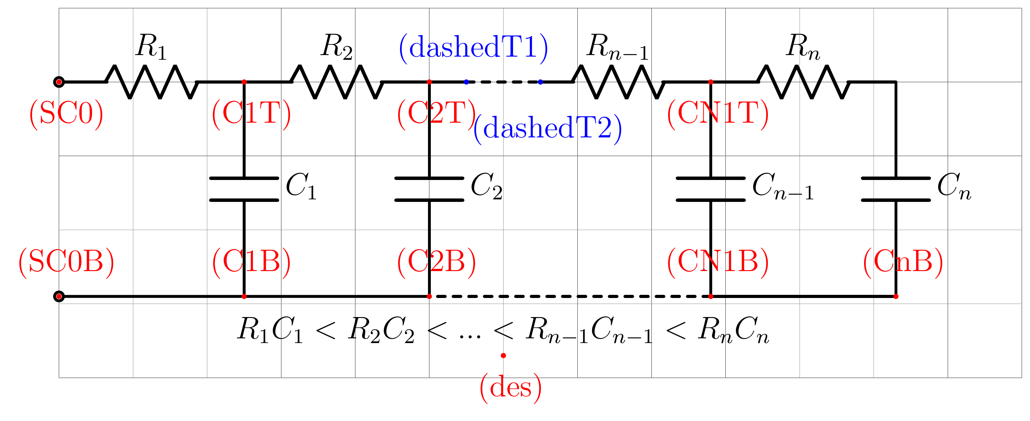

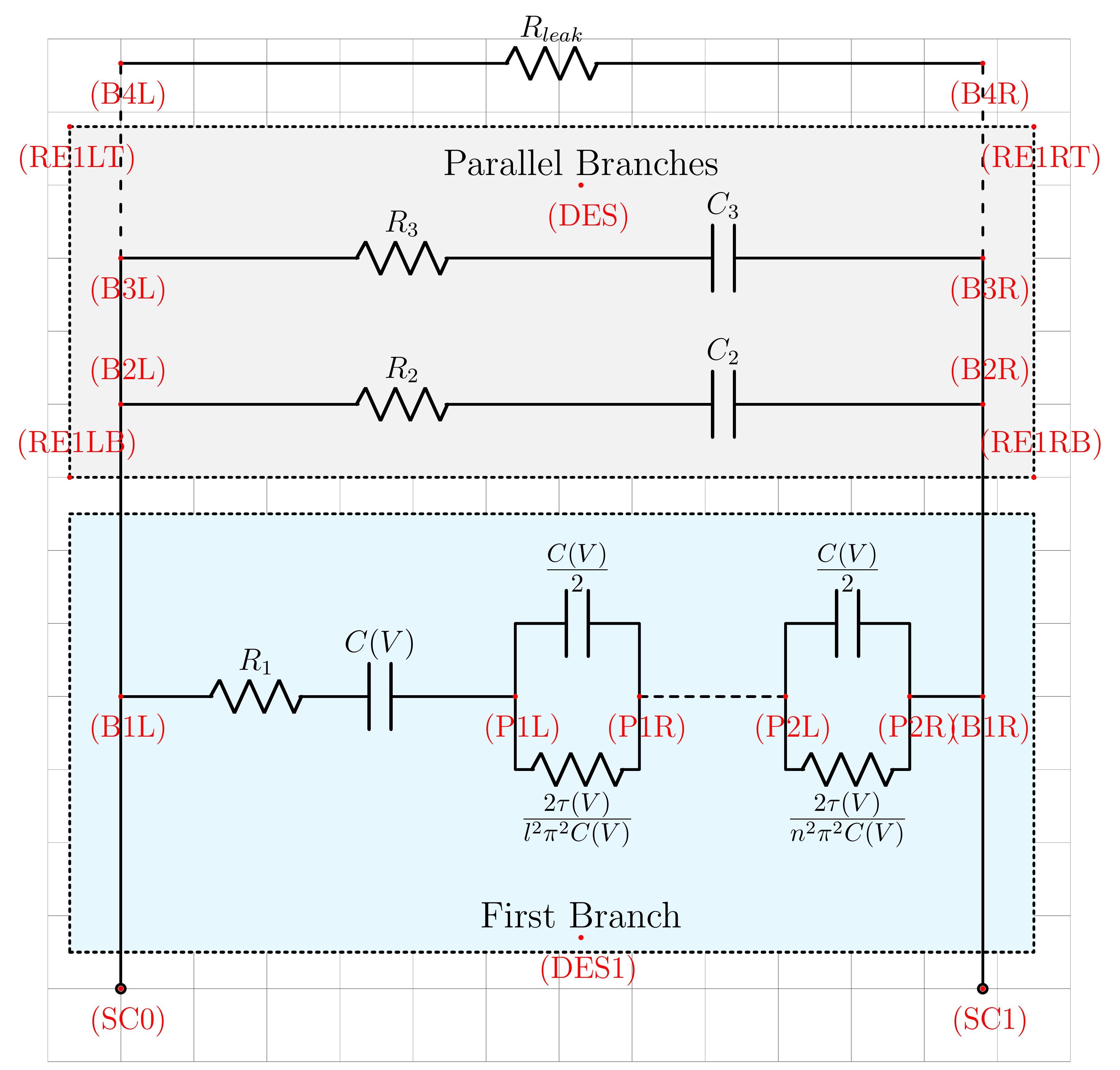
Well, we can see that, in more complicated cases, it’s more clearly to use the \coordinate command to label node and then use more \draw commands to connect them.
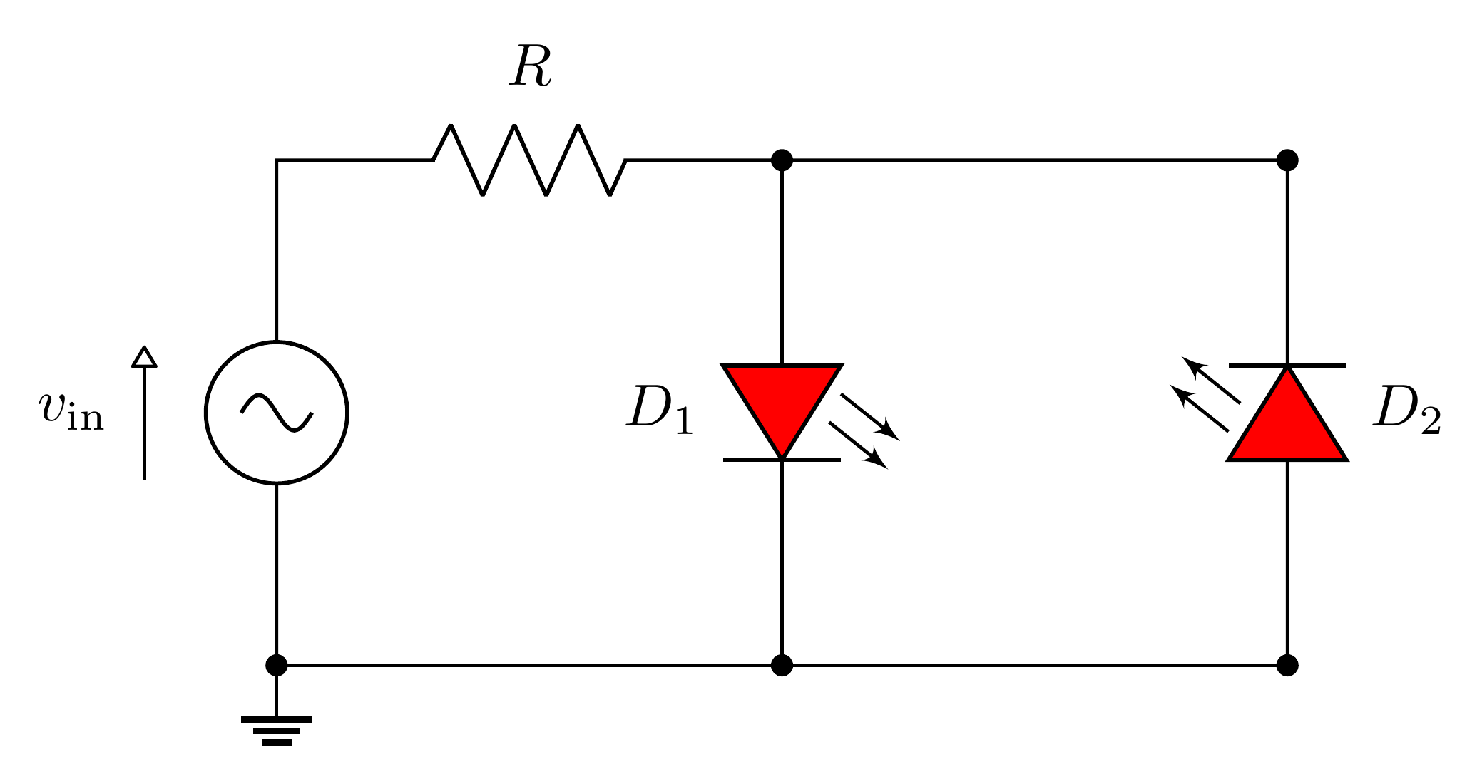
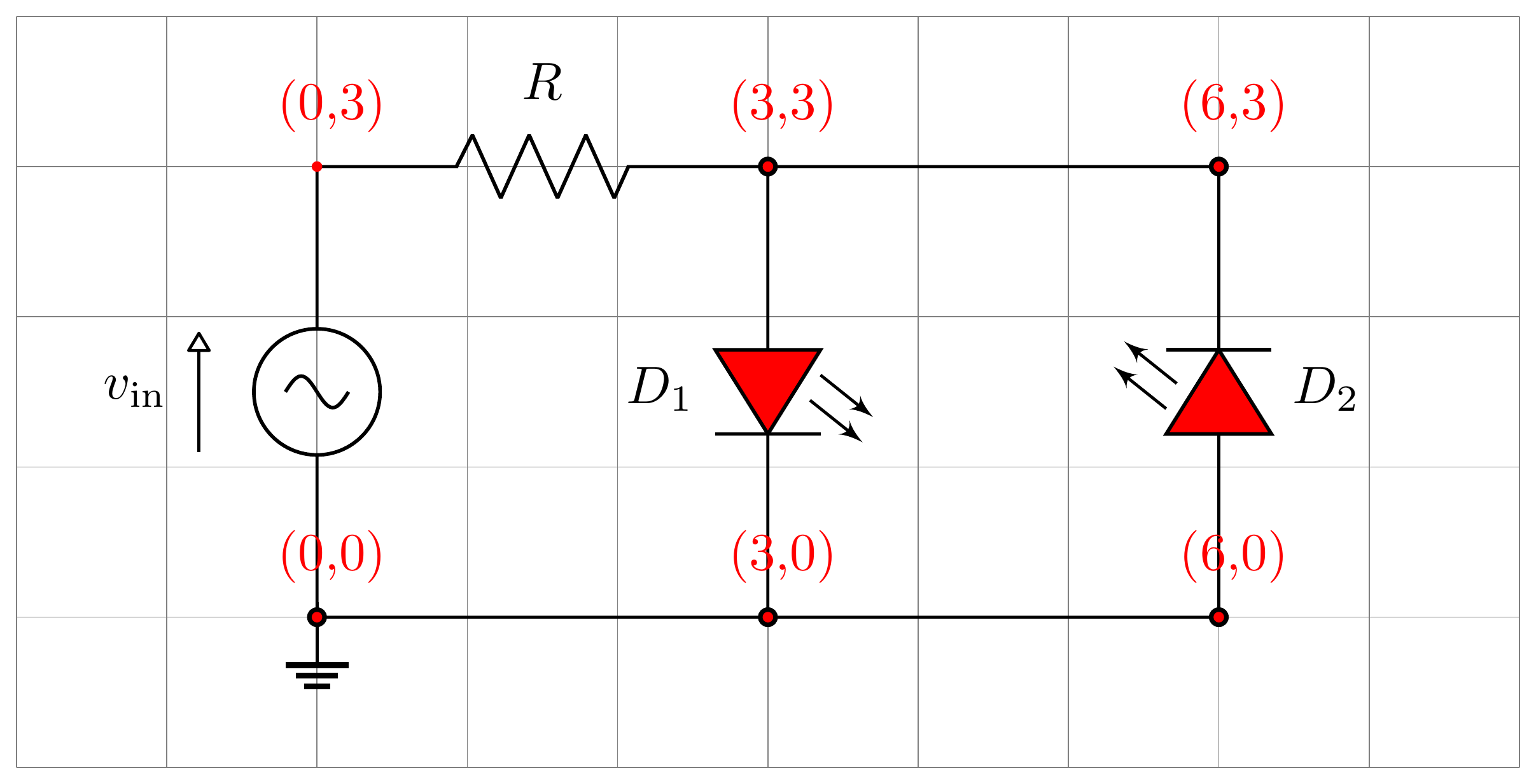
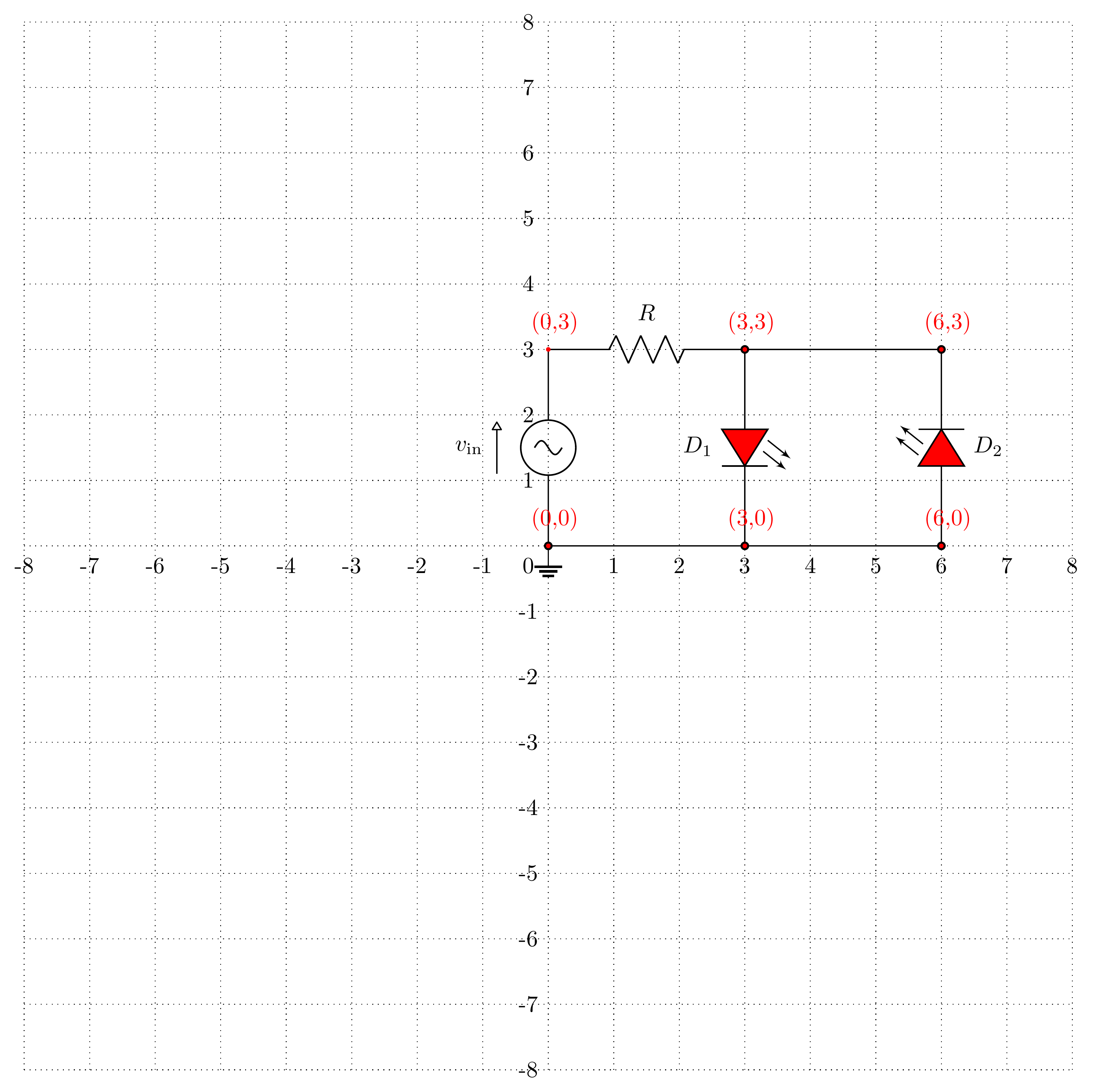
Example 5: LED – Diode Circuit
Example 5: LED – Diode Circuit10
1
2
3
4
5
6
7
8
9
10
11
12
13
14
15
16
17
18
19
20
21
22
23
24
25
26
27
28
29
30
31
32
33
34
35
36
37
38
39
40
41
42
43
44
45
46
47
48
49
50
51
52
53
54
55
56
57
58
59
60
61
\documentclass[border=3pt]{standalone}
\usepackage[european,s traightvoltages, RPvoltages, americanresistor, americaninductors]{circuitikz}
\tikzset{every picture/.style={line width=0.2mm}}
\usepackage{amsmath}
\usetikzlibrary{calc}
\ctikzset{bipoles/thickness=1.2, label distance=1mm, voltage shift = 1}

% Arrows Above Compenents
% Source: https://tex.stackexchange.com/questions/574576/circuitikz-straight-voltage-arrows-with-fixed-length
\newcommand{\fixedvlen}[3][0.4cm]{ % [semilength]{node}{label}
    % get the center of the standard arrow
    \coordinate (#2-Vcenter) at ($(#2-Vfrom)!0.5!(#2-Vto)$);
    % draw an arrow of a fixed size around that center and on the same line
    \draw[-{Triangle[round,open]}] ($(#2-Vcenter)!#1!(#2-Vfrom)$) -- ($(#2-Vcenter)!#1!(#2-Vto)$);
    % position the label as it where if standard voltages were used
    \node[ anchor=\ctikzgetanchor{#2}{Vlab}] at (#2-Vlab) {#3};
}

\newcommand{\fixedvlendashed}[3][0.75cm]{ % [semilength]{node}{label}
    % get the center of the standard arrow
    \coordinate (#2-Vcenter) at ($(#2-Vfrom)!0.5!(#2-Vto)$);
    % draw an arrow of a fixed size around that center and on the same line
    \draw[dashed,-{Triangle[round,open]}] ($(#2-Vcenter)!#1!(#2-Vfrom)$) -- ($(#2-Vcenter)!#1!(#2-Vto)$);
    % position the label as it where if standard voltages were used
    \node[ anchor=\ctikzgetanchor{#2}{Vlab}] at (#2-Vlab) {#3};
}

\begin{document}
\begin{circuitikz}
%	%Grid
%	\def\length{8}
%	\draw[thin, dotted] (-\length,-\length) grid (\length,\length);
%	\foreach \i in {1,...,\length}
%	{
%		\node at (\i,-2ex) {\i};
%		\node at (-\i,-2ex) {-\i};
%	}
%	\foreach \i in {1,...,\length}
%	{
%		\node at (-2ex,\i) {\i};
%		\node at (-2ex,-\i) {-\i};
%	}
%	\node at (-2ex,-2ex) {0};

	% Circuit
	\def\x{6}
	\def\y{3}
	\draw
	(0,0) to [sV, v>, name=v_in] (0,\y)
		to [R, l=$R$] (0.5*\x,\y)
		to [led, fill=red, l_=$D_1$, *-*] (0.5*\x,0) -- (0,0)
	(0.5*\x,\y) -- (\x,\y)
	(0.5*\x,0) -- (\x,0)
		to [led, fill=red, l_=$D_2$, *-*] (\x,\y)
	(0,0) to [short,*-] (0,0.1) node[ground] {};

	% Voltages
	\fixedvlen[0.4cm]{v_in}{$v_\text{in}$}
	% \fixedvlendashed[0.4cm]{v_in}{$v_\text{in}$}
\end{circuitikz}
\end{document}
Here is an annotated version:
1
2
3
4
5
6
7
8
9
10
11
12
13
14
15
16
17
18
19
20
21
22
23
24
25
26
27
28
29
30
31
32
33
34
35
36
37
38
39
40
41
42
43
44
45
46
47
48
49
50
51
52
53
54
55
56
57
58
59
60
61
62
63
64
65
66
67
68
69
70
\documentclass[border=3pt]{standalone}
\usepackage[european,s traightvoltages, RPvoltages, americanresistor, americaninductors]{circuitikz}
\tikzset{every picture/.style={line width=0.2mm}}
\usepackage{amsmath}
\usetikzlibrary{calc}
\ctikzset{bipoles/thickness=1.2, label distance=1mm, voltage shift = 1}

% Arrows Above Compenents
% Source: https://tex.stackexchange.com/questions/574576/circuitikz-straight-voltage-arrows-with-fixed-length
\newcommand{\fixedvlen}[3][0.4cm]{ % [semilength]{node}{label}
    % get the center of the standard arrow
    \coordinate (#2-Vcenter) at ($(#2-Vfrom)!0.5!(#2-Vto)$);
    % draw an arrow of a fixed size around that center and on the same line
    \draw[-{Triangle[round,open]}] ($(#2-Vcenter)!#1!(#2-Vfrom)$) -- ($(#2-Vcenter)!#1!(#2-Vto)$);
    % position the label as it where if standard voltages were used
    \node[ anchor=\ctikzgetanchor{#2}{Vlab}] at (#2-Vlab) {#3};
}

\newcommand{\fixedvlendashed}[3][0.75cm]{ % [semilength]{node}{label}
    % get the center of the standard arrow
    \coordinate (#2-Vcenter) at ($(#2-Vfrom)!0.5!(#2-Vto)$);
    % draw an arrow of a fixed size around that center and on the same line
    \draw[dashed,-{Triangle[round,open]}] ($(#2-Vcenter)!#1!(#2-Vfrom)$) -- ($(#2-Vcenter)!#1!(#2-Vto)$);
    % position the label as it where if standard voltages were used
    \node[ anchor=\ctikzgetanchor{#2}{Vlab}] at (#2-Vlab) {#3};
}

\begin{document}
\begin{circuitikz}
%	%Grid
%	\def\length{8}
%	\draw[thin, dotted] (-\length,-\length) grid (\length,\length);
%	\foreach \i in {1,...,\length}
%	{
%		\node at (\i,-2ex) {\i};
%		\node at (-\i,-2ex) {-\i};
%	}
%	\foreach \i in {1,...,\length}
%	{
%		\node at (-2ex,\i) {\i};
%		\node at (-2ex,-\i) {-\i};
%	}
%	\node at (-2ex,-2ex) {0};

	\draw [help lines,step=1cm] (-2,-1) grid (8,4); % Helper lines on the background

	% Circuit
	\def\x{6}
	\def\y{3}
	\draw
	(0,0) to [sV, v>, name=v_in] (0,\y)
		to [R, l=$R$] (0.5*\x,\y)
		to [led, fill=red, l_=$D_1$, *-*] (0.5*\x,0) -- (0,0)
	(0.5*\x,\y) -- (\x,\y)
	(0.5*\x,0) -- (\x,0)
		to [led, fill=red, l_=$D_2$, *-*] (\x,\y)
	(0,0) to [short,*-] (0,0.1) node[ground] {};

	% Voltages
	\fixedvlen[0.4cm]{v_in}{$v_\text{in}$}
	% \fixedvlendashed[0.4cm]{v_in}{$v_\text{in}$}

	\fill [red] (0,0) circle (1pt) node[right=0.1cm, above=0.1cm]{(0,0)};
	\fill [red] (0,3) circle (1pt) node[right=0.1cm, above=0.1cm]{(0,3)};
	\fill [red] (3,3) circle (1pt) node[right=0.1cm, above=0.1cm]{(3,3)};
	\fill [red] (6,3) circle (1pt) node[right=0.1cm, above=0.1cm]{(6,3)};
	\fill [red] (3,0) circle (1pt) node[right=0.1cm, above=0.1cm]{(3,0)};
	\fill [red] (6,0) circle (1pt) node[right=0.1cm, above=0.1cm]{(6,0)};
\end{circuitikz}
\end{document}
Actually, the author also provides a way to draw a grid background (the commented part), which method is basically the same as mine, but besides grid, it also can display x- and y-coordinate by using \foreach command:
1
2
3
4
5
6
7
8
9
10
11
12
13
14
15
16
17
18
19
20
21
22
23
24
25
26
27
28
29
30
31
32
33
34
35
36
37
38
39
40
41
42
43
44
45
46
47
48
49
50
51
52
53
54
55
56
57
58
59
60
61
62
63
64
65
66
67
68
 \documentclass[border=3pt]{standalone}
 \usepackage[european,s traightvoltages, RPvoltages, americanresistor, americaninductors]{circuitikz}
 \tikzset{every picture/.style={line width=0.2mm}}
 \usepackage{amsmath}
 \usetikzlibrary{calc}
 \ctikzset{bipoles/thickness=1.2, label distance=1mm, voltage shift = 1}

 % Arrows Above Compenents
 % Source: https://tex.stackexchange.com/questions/574576/circuitikz-straight-voltage-arrows-with-fixed-length
 \newcommand{\fixedvlen}[3][0.4cm]{ % [semilength]{node}{label}
     % get the center of the standard arrow
     \coordinate (#2-Vcenter) at ($(#2-Vfrom)!0.5!(#2-Vto)$);
     % draw an arrow of a fixed size around that center and on the same line
     \draw[-{Triangle[round,open]}] ($(#2-Vcenter)!#1!(#2-Vfrom)$) -- ($(#2-Vcenter)!#1!(#2-Vto)$);
     % position the label as it where if standard voltages were used
     \node[ anchor=\ctikzgetanchor{#2}{Vlab}] at (#2-Vlab) {#3};
 }

 \newcommand{\fixedvlendashed}[3][0.75cm]{ % [semilength]{node}{label}
     % get the center of the standard arrow
     \coordinate (#2-Vcenter) at ($(#2-Vfrom)!0.5!(#2-Vto)$);
     % draw an arrow of a fixed size around that center and on the same line
     \draw[dashed,-{Triangle[round,open]}] ($(#2-Vcenter)!#1!(#2-Vfrom)$) -- ($(#2-Vcenter)!#1!(#2-Vto)$);
     % position the label as it where if standard voltages were used
     \node[ anchor=\ctikzgetanchor{#2}{Vlab}] at (#2-Vlab) {#3};
 }

 \begin{document}
 \begin{circuitikz}
 	%Grid
 	\def\length{8}
 	\draw[thin, dotted] (-\length,-\length) grid (\length,\length);
 	\foreach \i in {1,...,\length}
 	{
 		\node at (\i,-2ex) {\i};
 		\node at (-\i,-2ex) {-\i};
 	}
 	\foreach \i in {1,...,\length}
 	{
 		\node at (-2ex,\i) {\i};
 		\node at (-2ex,-\i) {-\i};
 	}
 	\node at (-2ex,-2ex) {0};

 	% Circuit
 	\def\x{6}
 	\def\y{3}
 	\draw
 	(0,0) to [sV, v>, name=v_in] (0,\y)
 		to [R, l=$R$] (0.5*\x,\y)
 		to [led, fill=red, l_=$D_1$, *-*] (0.5*\x,0) -- (0,0)
 	(0.5*\x,\y) -- (\x,\y)
 	(0.5*\x,0) -- (\x,0)
 		to [led, fill=red, l_=$D_2$, *-*] (\x,\y)
 	(0,0) to [short,*-] (0,0.1) node[ground] {};

 	% Voltages
 	\fixedvlen[0.4cm]{v_in}{$v_\text{in}$}
 	% \fixedvlendashed[0.4cm]{v_in}{$v_\text{in}$}

 	\fill [red] (0,0) circle (1pt) node[right=0.1cm, above=0.1cm]{(0,0)};
 	\fill [red] (0,3) circle (1pt) node[right=0.1cm, above=0.1cm]{(0,3)};
 	\fill [red] (3,3) circle (1pt) node[right=0.1cm, above=0.1cm]{(3,3)};
 	\fill [red] (6,3) circle (1pt) node[right=0.1cm, above=0.1cm]{(6,3)};
 	\fill [red] (3,0) circle (1pt) node[right=0.1cm, above=0.1cm]{(3,0)};
 	\fill [red] (6,0) circle (1pt) node[right=0.1cm, above=0.1cm]{(6,0)};
 \end{circuitikz}
 \end{document}
A very elegant way!
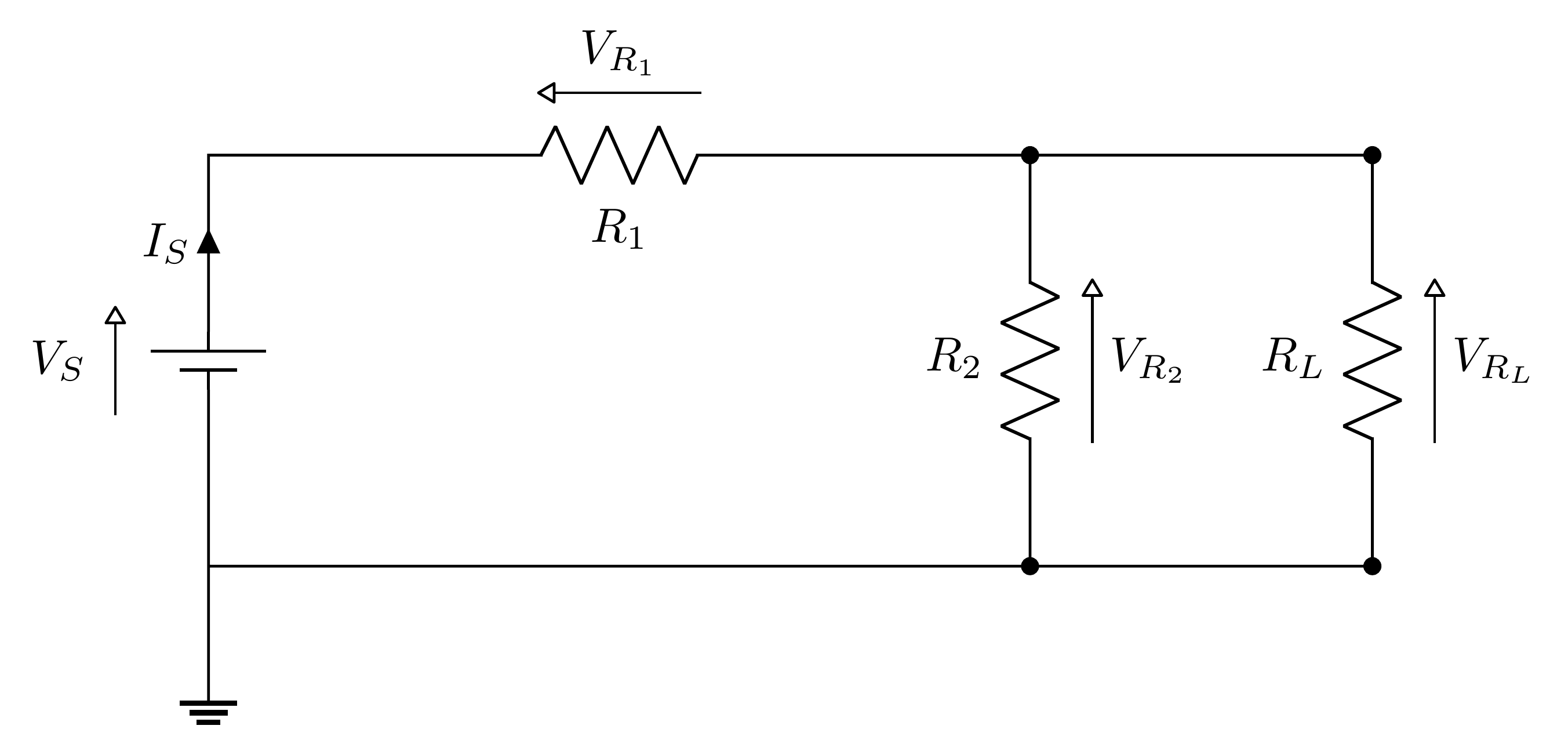
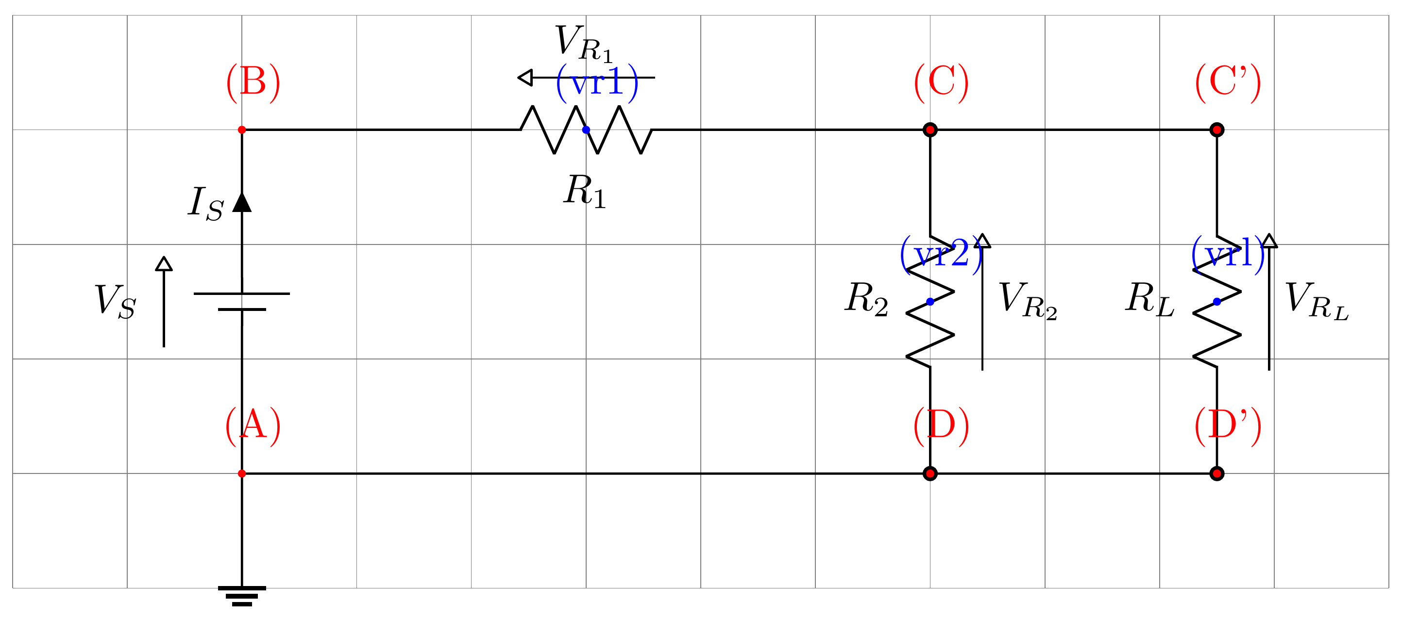
Example 6: Voltage Divider with Load
Example 6: Voltage Divider with Load11
1
2
3
4
5
6
7
8
9
10
11
12
13
14
15
16
17
18
19
20
21
22
23
24
25
26
27
28
29
30
31
32
33
34
35
36
37
38
39
40
41
42
43
44
45
46
47
48
49
50
51
52
53
54
55
56
57
58
59
60
61
62
63
64
\documentclass[border=3pt]{standalone}
\usepackage[european,s traightvoltages, RPvoltages, americanresistor, americaninductors]{circuitikz}
\tikzset{every picture/.style={line width=0.2mm}}
\usepackage{amsmath}
\usetikzlibrary{calc}
\ctikzset{bipoles/thickness=1.2, label distance=1mm, voltage shift = 1}

% Arrows Above Compenents
% Source: https://tex.stackexchange.com/questions/574576/circuitikz-straight-voltage-arrows-with-fixed-length
\newcommand{\fixedvlen}[3][0.4cm]{ % [semilength]{node}{label}
    % get the center of the standard arrow
    \coordinate (#2-Vcenter) at ($(#2-Vfrom)!0.5!(#2-Vto)$);
    % draw an arrow of a fixed size around that center and on the same line
    \draw[-{Triangle[round,open]}] ($(#2-Vcenter)!#1!(#2-Vfrom)$) -- ($(#2-Vcenter)!#1!(#2-Vto)$);
    % position the label as it where if standard voltages were used
    \node[ anchor=\ctikzgetanchor{#2}{Vlab}] at (#2-Vlab) {#3};
}
\newcommand{\fixedvlendashed}[3][0.75cm]{ % [semilength]{node}{label}
    % get the center of the standard arrow
    \coordinate (#2-Vcenter) at ($(#2-Vfrom)!0.5!(#2-Vto)$);
    % draw an arrow of a fixed size around that center and on the same line
    \draw[dashed,-{Triangle[round,open]}] ($(#2-Vcenter)!#1!(#2-Vfrom)$) -- ($(#2-Vcenter)!#1!(#2-Vto)$);
    % position the label as it where if standard voltages were used
    \node[ anchor=\ctikzgetanchor{#2}{Vlab}] at (#2-Vlab) {#3};
}

\begin{document}

\begin{circuitikz}
%	% Grid
%	\draw[thin, dotted] (0,0) grid (8,8);
%	\foreach \i in {1,...,8}
%	{
%		\node at (\i,-2ex) {\i};
%	}
%	\foreach \i in {1,...,8}
%	{
%		\node at (-2ex,\i) {\i};
%	}
%	\node at (-2ex,-2ex) {0};

	%C oordinates
	\coordinate (Earth) at (0,-1);
	\coordinate (A) at (0,0);
	\coordinate (B) at (0,3);
	\coordinate (C) at (6,3);
	\coordinate (D) at (6,0);
	\coordinate (C') at (8.5,3);
	\coordinate (D') at (8.5,0);

	% Circuit
	\draw (Earth) node[tlground]{} -- (A) to[battery1, i=$I_S$, v>, name=vs] (B)
			to[R, l_=$R_1$, v^<, name=vr1] (C)
			to [R, l_=$R_2$, v^<, name=vr2, *-*] (D) -- (A);
	\draw (C) -- (C') to[R, l_=$R_L$, v^<, name=vrl, *-*] (D') -- (D);

	% Voltages
	\fixedvlen[0.4cm]{vs}{$V_S$}
	\fixedvlen[0.6cm]{vr1}{$V_{R_1}$}
	\fixedvlen[0.6cm]{vr2}{$V_{R_2}$}
	\fixedvlen[0.6cm]{vrl}{$V_{R_L}$}
\end{circuitikz}

\end{document}
Here is an annotated version:
1
2
3
4
5
6
7
8
9
10
11
12
13
14
15
16
17
18
19
20
21
22
23
24
25
26
27
28
29
30
31
32
33
34
35
36
37
38
39
40
41
42
43
44
45
46
47
48
49
50
51
52
53
54
55
56
57
58
59
60
61
62
63
64
65
66
67
68
69
70
71
72
73
74
75
76
\documentclass[border=3pt]{standalone}
\usepackage[european,s traightvoltages, RPvoltages, americanresistor, americaninductors]{circuitikz}
\tikzset{every picture/.style={line width=0.2mm}}
\usepackage{amsmath}
\usetikzlibrary{calc}
\ctikzset{bipoles/thickness=1.2, label distance=1mm, voltage shift = 1}

% Arrows Above Compenents
% Source: https://tex.stackexchange.com/questions/574576/circuitikz-straight-voltage-arrows-with-fixed-length
\newcommand{\fixedvlen}[3][0.4cm]{ % [semilength]{node}{label}
    % get the center of the standard arrow
    \coordinate (#2-Vcenter) at ($(#2-Vfrom)!0.5!(#2-Vto)$);
    % draw an arrow of a fixed size around that center and on the same line
    \draw[-{Triangle[round,open]}] ($(#2-Vcenter)!#1!(#2-Vfrom)$) -- ($(#2-Vcenter)!#1!(#2-Vto)$);
    % position the label as it where if standard voltages were used
    \node[ anchor=\ctikzgetanchor{#2}{Vlab}] at (#2-Vlab) {#3};
}
\newcommand{\fixedvlendashed}[3][0.75cm]{ % [semilength]{node}{label}
    % get the center of the standard arrow
    \coordinate (#2-Vcenter) at ($(#2-Vfrom)!0.5!(#2-Vto)$);
    % draw an arrow of a fixed size around that center and on the same line
    \draw[dashed,-{Triangle[round,open]}] ($(#2-Vcenter)!#1!(#2-Vfrom)$) -- ($(#2-Vcenter)!#1!(#2-Vto)$);
    % position the label as it where if standard voltages were used
    \node[ anchor=\ctikzgetanchor{#2}{Vlab}] at (#2-Vlab) {#3};
}

\begin{document}

\begin{circuitikz}
%	%Grid
%	\draw[thin, dotted] (0,0) grid (8,8);
%	\foreach \i in {1,...,8}
%	{
%		\node at (\i,-2ex) {\i};
%	}
%	\foreach \i in {1,...,8}
%	{
%		\node at (-2ex,\i) {\i};
%	}
%	\node at (-2ex,-2ex) {0};
	\draw [help lines,step=1cm] (-2,-1) grid (10,4); % Helper lines on the background

	% Coordinates
	\coordinate (Earth) at (0,-1);
	\coordinate (A) at (0,0);
	\coordinate (B) at (0,3);
	\coordinate (C) at (6,3);
	\coordinate (D) at (6,0);
	\coordinate (C') at (8.5,3);
	\coordinate (D') at (8.5,0);

	% Circuit
	\draw (Earth) node[tlground]{} -- (A) to[battery1, i=$I_S$, v>, name=vs] (B)
			to [R, l_=$R_1$, v^<, name=vr1] (C)
			to [R, l_=$R_2$, v^<, name=vr2, *-*] (D) -- (A);
	\draw (C) -- (C') to[R, l_=$R_L$, v^<, name=vrl, *-*] (D') -- (D);

	% Voltages
	\fixedvlen[0.4cm]{vs}{$V_S$}
	\fixedvlen[0.6cm]{vr1}{$V_{R_1}$}
	\fixedvlen[0.6cm]{vr2}{$V_{R_2}$}
	\fixedvlen[0.6cm]{vrl}{$V_{R_L}$}

	\fill [red] (A) circle (1pt) node[right=0.1cm, above=0.1cm]{(A)};
	\fill [red] (B) circle (1pt) node[right=0.1cm, above=0.1cm]{(B)};
	\fill [red] (C) circle (1pt) node[right=0.1cm, above=0.1cm]{(C)};
	\fill [red] (D) circle (1pt) node[right=0.1cm, above=0.1cm]{(D)};
	\fill [red] (C') circle (1pt) node[right=0.1cm, above=0.1cm]{(C')};
	\fill [red] (D') circle (1pt) node[right=0.1cm, above=0.1cm]{(D')};

	\fill [blue] (vr1) circle (1pt) node[right=0.1cm, above=0.1cm]{(vr1)};
	\fill [blue] (vr2) circle (1pt) node[right=0.1cm, above=0.1cm]{(vr2)};
	\fill [blue] (vrl) circle (1pt) node[right=0.1cm, above=0.1cm]{(vrl)};
\end{circuitikz}

\end{document}
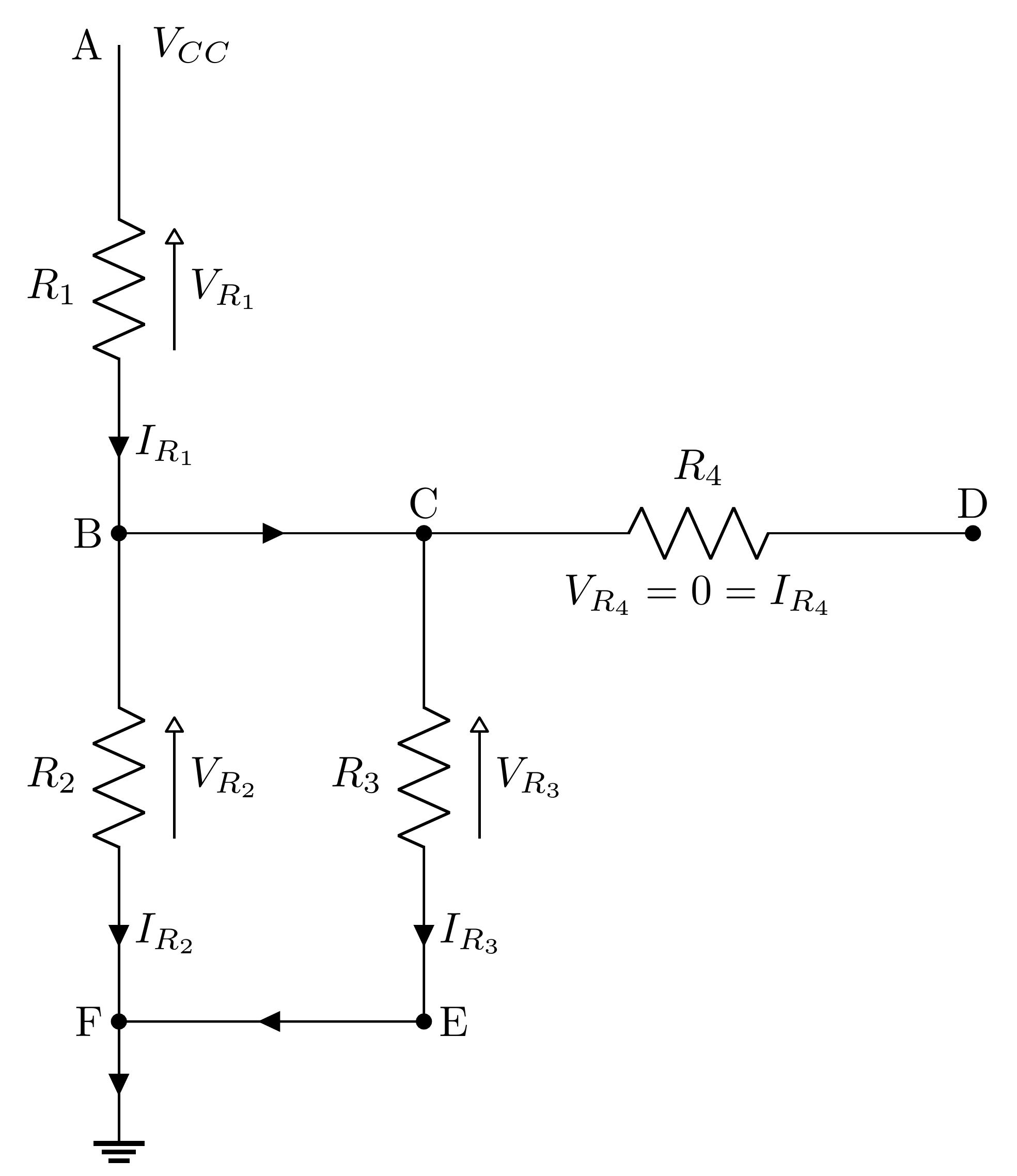
Example 7: Circuit with Resistors
Example 7: Circuit with Resistors12
1
2
3
4
5
6
7
8
9
10
11
12
13
14
15
16
17
18
19
20
21
22
23
24
25
26
27
28
29
30
31
32
33
34
35
36
37
38
39
40
41
42
43
44
45
46
47
48
49
50
51
52
53
54
55
56
57
58
59
60
61
62
63
64
65
66
67
68
69
70
71
72
\documentclass[border=3pt]{standalone}
\usepackage[european,s traightvoltages, RPvoltages, americanresistor, americaninductors]{circuitikz}
\tikzset{every picture/.style={line width=0.2mm}}
\usetikzlibrary{calc}
\usepackage{amsmath}
\ctikzset{bipoles/thickness=1.2, label distance=1mm, voltage shift = 1}

% Arrows Above Compenents
% Source: https://tex.stackexchange.com/questions/574576/circuitikz-straight-voltage-arrows-with-fixed-length
\newcommand{\fixedvlen}[3][0.4cm]{ % [semilength]{node}{label}
    % get the center of the standard arrow
    \coordinate (#2-Vcenter) at ($(#2-Vfrom)!0.5!(#2-Vto)$);
    % draw an arrow of a fixed size around that center and on the same line
    \draw[-{Triangle[round,open]}] ($(#2-Vcenter)!#1!(#2-Vfrom)$) -- ($(#2-Vcenter)!#1!(#2-Vto)$);
    % position the label as it where if standard voltages were used
    \node[ anchor=\ctikzgetanchor{#2}{Vlab}] at (#2-Vlab) {#3};
}
\newcommand{\fixedvlendashed}[3][0.75cm]{ % [semilength]{node}{label}
    % get the center of the standard arrow
    \coordinate (#2-Vcenter) at ($(#2-Vfrom)!0.5!(#2-Vto)$);
    % draw an arrow of a fixed size around that center and on the same line
    \draw[dashed,-{Triangle[round,open]}] ($(#2-Vcenter)!#1!(#2-Vfrom)$) -- ($(#2-Vcenter)!#1!(#2-Vto)$);
    % position the label as it where if standard voltages were used
    \node[ anchor=\ctikzgetanchor{#2}{Vlab}] at (#2-Vlab) {#3};
}

\begin{document}

\begin{circuitikz}
%	%Grid
%	\draw[thin, dotted] (0,0) grid (8,8);
%	\foreach \i in {1,...,8}
%	{
%		\node at (\i,-2ex) {\i};
%	}
%	\foreach \i in {1,...,8}
%	{
%		\node at (-2ex,\i) {\i};
%	}
%	\node at (-2ex,-2ex) {0};

	% Coordinates
	\coordinate (A) at (0,8);
	\coordinate (B) at (0,4);
	\coordinate (C) at (2.5,4);
	\coordinate (D) at (7,4);
	\coordinate (E) at (2.5,0);
	\coordinate (Z) at (0,0);
	\coordinate (Earth) at (0,-1);

	% Circuit
	\draw (A) to[resistor, l_=$R_1$, i>=$I_{R_1}$, v^<, name=r1] (B) to[short, i>=$$] (C)
		 to[resistor, l^=$R_4$, a_= {$V_{R_4}= 0 = I_{R_4}$}, name=r4, *-*] (D);
	\draw (B) to[resistor, l_=$R_2$, i>=$I_{R_2}$, v^<, name=r2, *-*] (Z) to[short, i>=$$] (Earth) node[tlground]{};
	\draw (C) to[resistor, l_=$R_3$, i>=$I_{R_3}$, v^<, name=r3, *-*] (E) to[short, i>=$$] (Z);

	% Nodes
	\node[shift={(0.6,0)}] at (A) {$V_{CC}$};
	\node[left] at (A) {A};
	\node[left] at (B) {B};
	\node[above] at (C) {C};
	\node[above] at (D) {D};
	\node[right] at (E) {E};
	\node[left] at (Z) {F};

	% Voltages
	\fixedvlen[0.5cm]{r1}{$V_{R_1}$}
	\fixedvlen[0.5cm]{r2}{$V_{R_2}$}
	\fixedvlen[0.5cm]{r3}{$V_{R_3}$}
\end{circuitikz}

\end{document}
Here is an annotated version:
1
2
3
4
5
6
7
8
9
10
11
12
13
14
15
16
17
18
19
20
21
22
23
24
25
26
27
28
29
30
31
32
33
34
35
36
37
38
39
40
41
42
43
44
45
46
47
48
49
50
51
52
53
54
55
56
57
58
59
60
61
62
63
64
65
66
67
68
69
70
71
72
73
74
75
76
77
78
\documentclass[border=3pt]{standalone}
\usepackage[european,s traightvoltages, RPvoltages, americanresistor, americaninductors]{circuitikz}
\tikzset{every picture/.style={line width=0.2mm}}
\usetikzlibrary{calc}
\usepackage{amsmath}
\ctikzset{bipoles/thickness=1.2, label distance=1mm, voltage shift = 1}

% Arrows Above Compenents
% Source: https://tex.stackexchange.com/questions/574576/circuitikz-straight-voltage-arrows-with-fixed-length
\newcommand{\fixedvlen}[3][0.4cm]{ % [semilength]{node}{label}
    % get the center of the standard arrow
    \coordinate (#2-Vcenter) at ($(#2-Vfrom)!0.5!(#2-Vto)$);
    % draw an arrow of a fixed size around that center and on the same line
    \draw[-{Triangle[round,open]}] ($(#2-Vcenter)!#1!(#2-Vfrom)$) -- ($(#2-Vcenter)!#1!(#2-Vto)$);
    % position the label as it where if standard voltages were used
    \node[ anchor=\ctikzgetanchor{#2}{Vlab}] at (#2-Vlab) {#3};
}
\newcommand{\fixedvlendashed}[3][0.75cm]{ % [semilength]{node}{label}
    % get the center of the standard arrow
    \coordinate (#2-Vcenter) at ($(#2-Vfrom)!0.5!(#2-Vto)$);
    % draw an arrow of a fixed size around that center and on the same line
    \draw[dashed,-{Triangle[round,open]}] ($(#2-Vcenter)!#1!(#2-Vfrom)$) -- ($(#2-Vcenter)!#1!(#2-Vto)$);
    % position the label as it where if standard voltages were used
    \node[ anchor=\ctikzgetanchor{#2}{Vlab}] at (#2-Vlab) {#3};
}

\begin{document}

\begin{circuitikz}
%	%Grid
%	\draw[thin, dotted] (0,0) grid (8,8);
%	\foreach \i in {1,...,8}
%	{
%		\node at (\i,-2ex) {\i};
%	}
%	\foreach \i in {1,...,8}
%	{
%		\node at (-2ex,\i) {\i};
%	}
%	\node at (-2ex,-2ex) {0};

	\draw [help lines,step=1cm] (-2,-1) grid (8,8); % Helper lines on the background

	% Coordinates
	\coordinate (A) at (0,8);
	\coordinate (B) at (0,4);
	\coordinate (C) at (2.5,4);
	\coordinate (D) at (7,4);
	\coordinate (E) at (2.5,0);
	\coordinate (Z) at (0,0);
	\coordinate (Earth) at (0,-1);

	% Circuit
	\draw (A) to [resistor, l_=$R_1$, i>=$I_{R_1}$, v^<, name=r1] (B) to [short, i>=$ $] (C)
		 to [resistor, l^=$R_4$, a_= {$V_{R_4}= 0 = I_{R_4}$}, name=r4, *-*] (D);
	\draw (B) to [resistor, l_=$R_2$, i>=$I_{R_2}$, v^<, name=r2, *-*] (Z) to [short, i>=$ $] (Earth) node[tlground]{};
	\draw (C) to [resistor, l_=$R_3$, i>=$I_{R_3}$, v^<, name=r3, *-*] (E) to [short, i>=$ $] (Z);

	% Nodes
	\node[shift={(0.6,0)}] at (A) {$V_{CC}$};
	\node[left] at (A) {A};
	\node[left] at (B) {B};
	\node[above] at (C) {C};
	\node[above] at (D) {D};
	\node[right] at (E) {E};
	\node[left] at (Z) {F};

	% Voltages
	\fixedvlen[0.5cm]{r1}{$V_{R_1}$}
	\fixedvlen[0.5cm]{r2}{$V_{R_2}$}
	\fixedvlen[0.5cm]{r3}{$V_{R_3}$}

	\fill [red] (r1) circle (1pt) node[right=0.1cm, above=0.1cm]{(r1)};
	\fill [red] (r2) circle (1pt) node[right=0.1cm, above=0.1cm]{(r2)};
	\fill [red] (r3) circle (1pt) node[right=0.1cm, above=0.1cm]{(r3)};
\end{circuitikz}

\end{document}

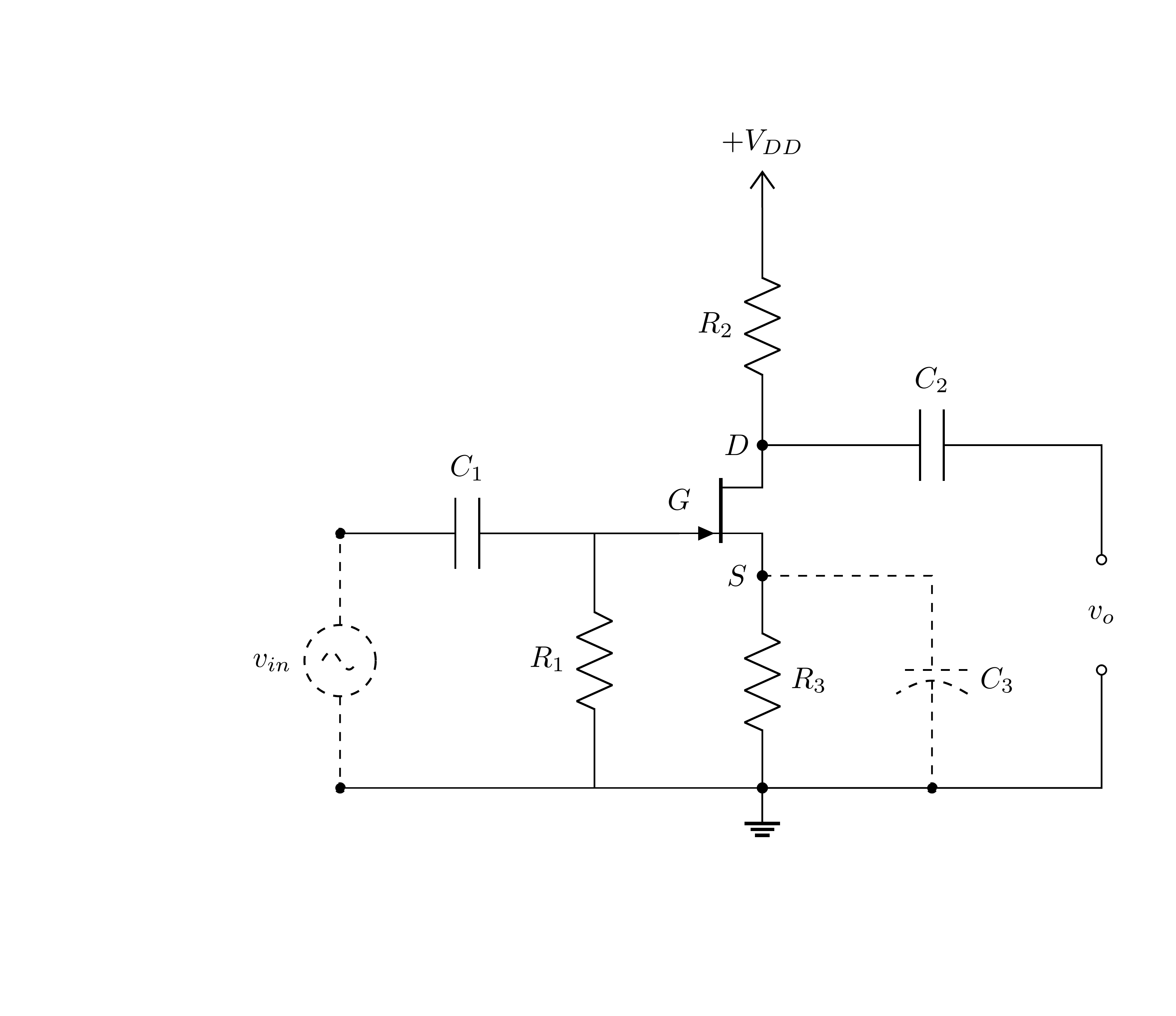
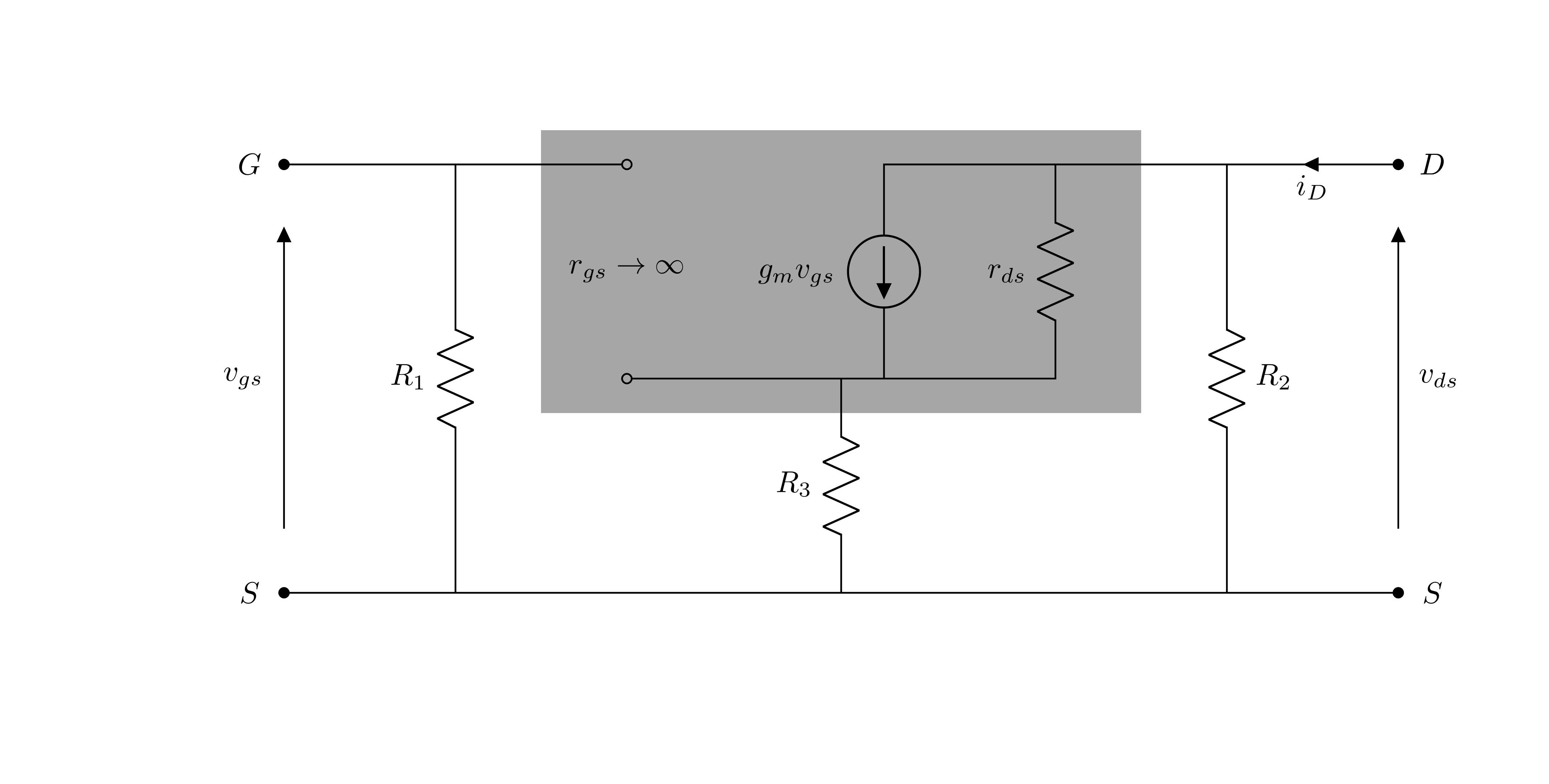
Example 8: JFET in Common Source Wiring and AC Equivalent
Example 8: JFET in Common Source Wiring and AC Equivalent13
1
2
3
4
5
6
7
8
9
10
11
12
13
14
15
16
17
18
19
20
21
22
23
24
25
26
27
28
29
30
31
32
33
34
35
36
37
38
39
40
41
42
43
44
45
46
47
48
49
50
51
52
53
54
55
56
57
58
59
60
61
62
63
64
65
66
67
68
69
70
71
72
73
74
75
76
77
78
79
80
81
82
83
84
85
86
87
88
89
90
91
92
93
94
95
96
97
98
99
100
101
102
\documentclass[border=50pt, tikz]{standalone}
\usepackage[european,s traightvoltages, RPvoltages, americanresistor, americaninductors]{circuitikz}
\tikzset{every picture/.style={line width=0.2mm}}
\usetikzlibrary{calc}
\ctikzset{bipoles/thickness=1.2, label distance=1mm, voltage shift = 1}

\def\nu{10}
\definecolor{myblue}{HTML}{ABDCEC}

\begin{document}

\begin{tikzpicture}
\begin{circuitikz}
	\ctikzset{voltage/american plus/.initial={}, voltage/american minus/.initial={}}

%	%Grid
%	\draw[thin, dotted] (0,0) grid (\nu,\nu);
%	\foreach \i in {1,...,\nu}
%	{
%		\node at (\i,-2ex) {\i};
%	}
%	\foreach \i in {1,...,\nu}
%	{
%		\node at (-2ex,\i) {\i};
%	}
%	\node at (-2ex,-2ex) {0};

	%Coordinates
	\node[njfet] (Q) at (5,3.5) {};

	% Circuit
	\draw

	(Q.S) node[shift={(-0.3,0)}] {$S$} to [R, l^=$R_3$, *-*] ++(0,-2.5) node[ground] (GR) {}

	(Q.D) node[shift={(-0.3,0)}] {$D$} to [R, l^=$R_2$, *-] ++(0,2.8) node[vcc] {$+V_{DD}$}
	(Q.D) to [C, l^=$C_2$] ++(4,0) -- ++(0,-1.35) node (D') {}
	to [open, v=$v_o$, o-o, american] ++(0,-1.3) -- (GR -| D') -- (GR)

	(Q.G) node[shift={(0,0.4)}] {$G$} -- ++(-1,0) node[inner sep=0, outer sep=-1] (G') {} to [R, l_=$R_1$] (GR -| G')
	(G') to[C, l_=$C_1$] ++(-3,0) node (G'') {};

	\draw (GR) -- (GR -| G'');

	\draw[dashed]
	(Q.S) -- ++(2,0) to[curved capacitor, l^=$C_3$, -*] ++(0,-2.5)
	(G'') to [sV, l_=$v_{in}$, *-*] (G'' |- GR);
\end{circuitikz}
\end{tikzpicture}

\begin{tikzpicture}
\begin{circuitikz}
	\ctikzset{voltage/american plus/.initial={}, voltage/american minus/.initial={}}

%	% Grid
%	\draw[thin, dotted] (0,0) grid (\nu,\nu);
%	\foreach \i in {1,...,\nu}
%	{
%		\node at (\i,-2ex) {\i};
%	}
%	\foreach \i in {1,...,\nu}
%	{
%		\node at (-2ex,\i) {\i};
%	}
%	\node at (-2ex,-2ex) {0};

	% Coordinates
	\coordinate (G) at (0,5);
	\coordinate (S) at (0,0);

	% Circuit
	\draw

	% Left Part
	(G) node[shift={(-0.4,0)}] {$G$} to [open, v_=$v_{gs}$, *-*] (S) node[shift={(-0.4, 0)}] {$S$}
	(G) -- ++(4,0) coordinate (G) to [open, v=$r_{gs}\to\infty$, o-o, american] ++(0,-2.5) coordinate (ML)

	(S) -- ++(2,0) coordinate (SL) to [R, l^=$R_1$] (SL |- G) coordinate (G')

	(SL) -- ++(2,0)

	% Right Part
	(ML) -- ++ (3,0) coordinate (MR) to [american current source, l^=$g_mv_{gs}$, invert] ++(0,2.5)
	-- ++(6,0) coordinate (D) node[shift={(0.4, 0)}] {$D$}

	(MR) -- ++(2,0) coordinate (MR') to [R, l^=$r_{ds}$] (MR' |- D) coordinate (D'')

	($(ML)!0.5!(MR')$) to [R, l_=$R_3$] ++(0,-2.5) coordinate (SM) -- (S)

	(D'') -- ++(2,0) coordinate (D') to [R, l^=$R_2$] (D' |- S) coordinate (SR')

	(SR') -- (SR' -| D) coordinate (SR)
	(SR') -- (SM)

	(D) node[shift={(0.4,0)}] {$D$} to [open, v^=$v_{ds}$, *-*] (SR) node[shift={(0.4, 0)}] {$S$}
	(D) to [short, i=$i_{D}$] (D');

	% Rectangle
	\draw[draw=none, fill=black, fill opacity=0.35] ($(ML) - (1,0.4)$) rectangle ($(D'')!0.5!(D') + (0,0.4)$);
\end{circuitikz}
\end{tikzpicture}
\end{document}
Here is an annotated version:
1
2
3
4
5
6
7
8
9
10
11
12
13
14
15
16
17
18
19
20
21
22
23
24
25
26
27
28
29
30
31
32
33
34
35
36
37
38
39
40
41
42
43
44
45
46
47
48
49
50
51
52
53
54
55
56
57
58
59
60
61
62
63
64
65
66
67
68
69
70
71
72
73
74
75
76
77
78
79
80
81
82
83
84
85
86
87
88
89
90
91
92
93
94
95
96
97
98
99
100
101
102
103
104
105
106
107
108
109
110
111
112
113
114
115
116
\documentclass[border=50pt, tikz]{standalone}
\usepackage[european,s traightvoltages, RPvoltages, americanresistor, americaninductors]{circuitikz}
\tikzset{every picture/.style={line width=0.2mm}}
\usetikzlibrary{calc}
\ctikzset{bipoles/thickness=1.2, label distance=1mm, voltage shift = 1}

\def\nu{10}
\definecolor{myblue}{HTML}{ABDCEC}

\begin{document}

\begin{tikzpicture}
\begin{circuitikz}
	\ctikzset{voltage/american plus/.initial={}, voltage/american minus/.initial={}}

%	%Grid
%	\draw[thin, dotted] (0,0) grid (\nu,\nu);
%	\foreach \i in {1,...,\nu}
%	{
%		\node at (\i,-2ex) {\i};
%	}
%	\foreach \i in {1,...,\nu}
%	{
%		\node at (-2ex,\i) {\i};
%	}
%	\node at (-2ex,-2ex) {0};
	\draw [help lines,step=1cm] (-2,-1) grid (12,9); % Helper lines on the background

	%Coordinates
	\node[njfet] (Q) at (5,3.5) {};

	% Circuit
	\draw
		(Q.S) node[shift={(-0.3,0)}]{$S$} to [R, l^=$R_3$, *-*] ++(0,-2.5) node[ground](GR){}
		(Q.D) node[shift={(-0.3,0)}]{$D$} to [R, l^=$R_2$, *-] ++(0,2.8) node[vcc]{$+V_{DD}$}
		(Q.D) to [C, l^=$C_2$] ++(4,0) -- ++(0,-1.35) node(D'){}
		to [open, v=$v_o$, o-o, american] ++(0,-1.3) -- (GR -| D') -- (GR)
		(Q.G) node[shift={(0,0.4)}]{$G$} -- ++(-1,0) node[inner sep=0, outer sep=-1] (G') {} to [R, l_=$R_1$] (GR -| G')
		(G') to[C, l_=$C_1$] ++(-3,0) node(G''){};

	\draw (GR) -- (GR -| G'');

	\draw[dashed]
		(Q.S) -- ++(2,0) to[curved capacitor, l^=$C_3$, -*] ++(0,-2.5)
		(G'') to [sV, l_=$v_{in}$, *-*] (G'' |- GR);

	\fill [red] (Q) circle (1pt) node[right=0.1cm]{(Q)};
	\fill [red] (Q.S) circle (1pt) node[right=0.1cm, below=0.1cm]{(Q.S)};
	\fill [red] (Q.D) circle (1pt) node[right=0.1cm, above=0.1cm]{(Q.D)};
	\fill [red] (Q.G) circle (1pt) node[right=0.1cm, below=0.1cm]{(Q.G)};

	\fill [red] (GR) circle (1pt) node[right=0.1cm, above=0.1cm]{(GR)};
	\fill [red] (D') circle (1pt) node[right=0.1cm, above=0.1cm]{(D')};
	\fill [red] (G') circle (1pt) node[right=0.1cm, above=0.1cm]{(G')};
	\fill [red] (G'') circle (1pt) node[right=0.1cm, above=0.1cm]{(G'')};
\end{circuitikz}
\end{tikzpicture}

\begin{tikzpicture}
\begin{circuitikz}
	\ctikzset{voltage/american plus/.initial={}, voltage/american minus/.initial={}}

%	% Grid
%	\draw[thin, dotted] (0,0) grid (\nu,\nu);
%	\foreach \i in {1,...,\nu}
%	{
%		\node at (\i,-2ex) {\i};
%	}
%	\foreach \i in {1,...,\nu}
%	{
%		\node at (-2ex,\i) {\i};
%	}
%	\node at (-2ex,-2ex) {0};
	\draw [help lines,step=1cm] (-2,-1) grid (15,7); % Helper lines on the background

	% Coordinates
	\coordinate (G) at (0,5);
	\coordinate (S) at (0,0);

	% Circuit
	\draw
		% Left Part
		(G) node[shift={(-0.4,0)}] {$G$} to [open, v_=$v_{gs}$, *-*] (S) node[shift={(-0.4, 0)}]{$S$}
		(G) -- ++(4,0) coordinate (G) to [open, v=$r_{gs}\to\infty$, o-o, american] ++(0,-2.5) coordinate (ML) % The coordinates of G change here.
		(S) -- ++(2,0) coordinate (SL) to [R, l^=$R_1$] (SL |- G) coordinate (G')
		(SL) -- ++(2,0)
		% Right Part
		(ML) -- ++ (3,0) coordinate (MR) to [american current source, l^=$g_mv_{gs}$, invert] ++(0,2.5)
		-- ++(6,0) coordinate (D) node[shift={(0.4, 0)}] {$D$}
		(MR) -- ++(2,0) coordinate (MR') to [R, l^=$r_{ds}$] (MR' |- D) coordinate (D'')
		($(ML)!0.5!(MR')$) to [R, l_=$R_3$] ++(0,-2.5) coordinate (SM) -- (S)
		(D'') -- ++(2,0) coordinate (D') to [R, l^=$R_2$] (D' |- S) coordinate (SR')
		(SR') -- (SR' -| D) coordinate (SR)
		(SR') -- (SM)
		(D) node[shift={(0.4,0)}] {$D$} to [open, v^=$v_{ds}$, *-*] (SR) node[shift={(0.4, 0)}] {$S$}
		(D) to [short, i=$i_{D}$] (D');

	% Rectangle
	\draw[draw=none, fill=black, fill opacity=0.35] ($(ML) - (1,0.4)$) rectangle ($(D'')!0.5!(D') + (0,0.4)$);

	\fill [red] (G) circle (1pt) node[above=0.1cm]{(G)};
	\fill [red] (S) circle (1pt) node[below=0.1cm]{(S)};
	\fill [red] (ML) circle (1pt) node[below=0.1cm]{(ML)};
	\fill [red] (SL) circle (1pt) node[below=0.1cm]{(SL)};
	\fill [red] (G') circle (1pt) node[above=0.1cm]{(G')};
	\fill [red] (D) circle (1pt) node[above=0.1cm]{(D)};
	\fill [red] (D') circle (1pt) node[above=0.1cm]{(D')};
	\fill [red] (D'') circle (1pt) node[above=0.1cm]{(D'')};
	\fill [red] (MR) circle (1pt) node[below=0.1cm]{(MR)};
	\fill [red] (MR') circle (1pt) node[below=0.1cm]{(MR')};
	\fill [red] (SR) circle (1pt) node[below=0.1cm]{(SR)};
	\fill [red] (SR') circle (1pt) node[below=0.1cm]{(SR')};
	\fill [red] (SM) circle (1pt) node[below=0.1cm]{(SM)};
\end{circuitikz}
\end{tikzpicture}
\end{document}

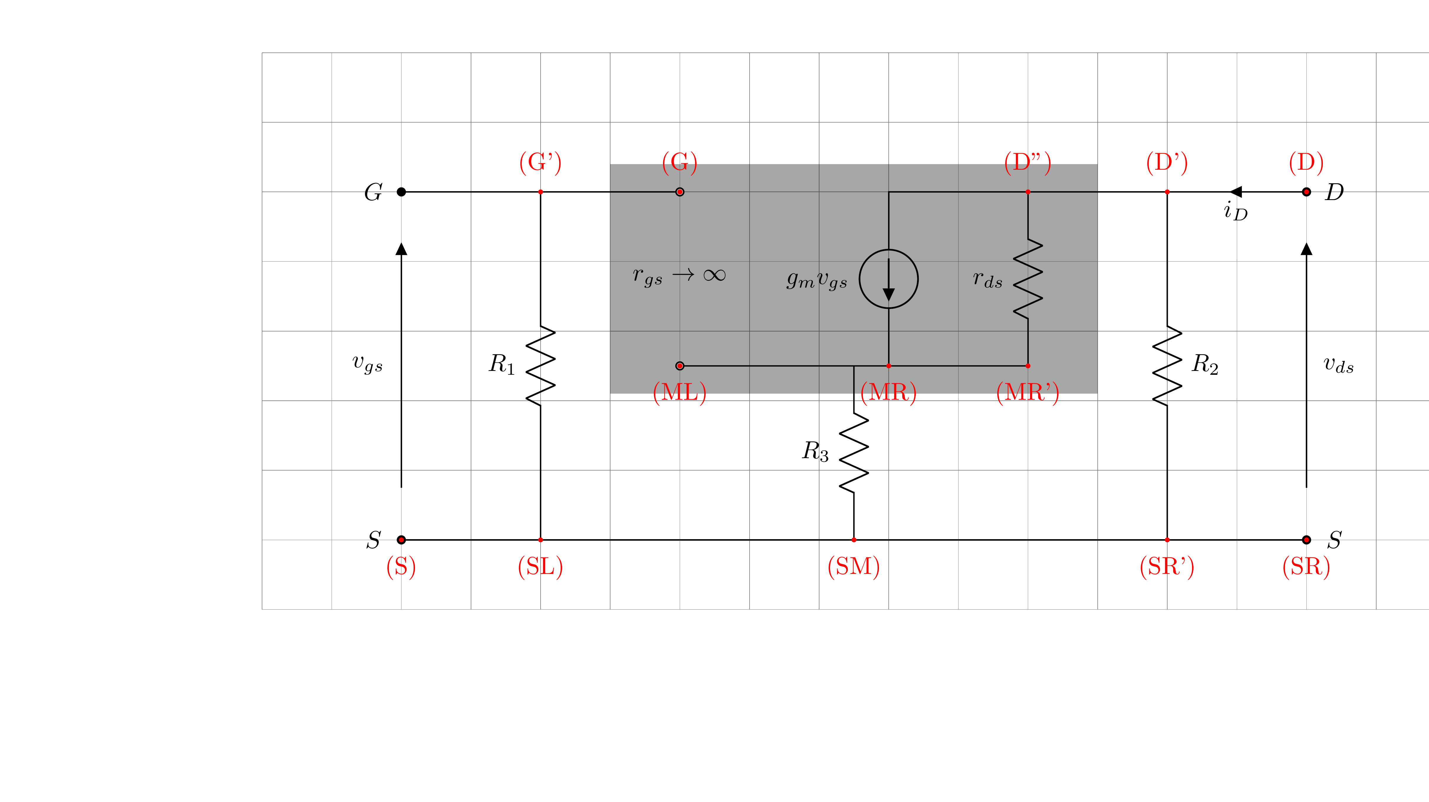
In this example, note that:
- how to specify the coordinates by the intersection of perpendicular lines, like
(SL |- G)etc.8; - how to calculate the position of the rectangle based on existing coordinates,
\draw[draw=none, fill=black, fill opacity=0.35] ($(ML) - (1,0.4)$) rectangle ($(D'')!0.5!(D') + (0,0.4)$);.
References